Light emitting device

a technology of light emitting devices and light emitting surfaces, which is applied in the manufacture of semiconductor/solid-state devices, semiconductor structures, electrical devices, etc., can solve the problems of low manufacturing throughput low manufacturing throughput associated with small substrate dimensions, and high cost of conventional solid-state light emitting devices. , to achieve the effect of reducing absorption-related light loss, increasing light emission intensity, and increasing light emission intensity

Inactive Publication Date: 2009-02-05
SIPHOTON
View PDF14 Cites 98 Cited by
  • Summary
  • Abstract
  • Description
  • Claims
  • Application Information

AI Technical Summary

Benefits of technology

[0016]An advantage associated with the disclosed light emitting device is that it significantly increases light emission intensity comparing to conventional LED light emitting devices. The disclosed light emitting devices and methods provide much larger light emitting surface than conventional LED light emitting devices having the same substrate foot print. A reflective layer under the disclosed light emitting devices can decrease absorption-related light loss and further increase emission efficiency. A transparent conductive layer formed on the upper Group III-V compound layer of the disclosed light emitting device can increase electric contact between the upper electrode and the upper III-V layer, and at the same time, maximize light emission intensity from the disclosed light emitting device.
[0017]Another advantage associated with the disclosed light emitting device is that its light emission is focused in much narrower angular range than conventional LED light emitting devices. The more concentrated angular light emission in the disclosed light emitting device reduces the light loss to unwanted directions and can thus increase brightness in the intended illumination directions and reduce energy consumption.
[0018]Another advantage associated with the disclosed light emitting device is that it is more practical to manufacture, robust, and reliable than some conventional light emitting systems. The disclosed light emitting devices and fabrication processes can overcome differential thermal expansions and lattice mismatch between the lower group compound III-V layer and the substrate and prevent associated layer cracking and delamination, problems known in conventional LED lighting systems.
[0019]The disclosed light emitting device and fabrication processes allow for high-throughput and high-volume manufacturing of the light emitting devices. A large number of solid state LEDs can be fabricated on a large substrate such as a silicon wafer or a glass substrate. Manufacturing throughput can be much improved since silicon wafer can be provided in much larger dimensions (e.g. 6 to 12 inch silicon wafers) compared to the small substrates used in the conventional light emitting devices. The disclosed light emitting device can be fabricated using commercially available semiconductor processing equipment such as ALD and MOCVD systems without using customized fabrication equipments, which makes the disclosed manufacturing process easily implemented. The disclosed light emitting device can thus be fabricated more efficiently in cost and time than some conventional light emitting devices that need.
[0020]Furthermore, the disclosed light emitting devices can be made more integrated, compact, and cost effective compared to some conventional LED devices. The disclosed light emitting devices can be fabricated on a silicon-based substrate which allows the integration of electronic control circuitry in the substrate.

Problems solved by technology

Although solid-state lighting offers certain advantages, conventional semiconductor structures and devices used for solid-state lighting are relatively expensive.
One of the costs related to conventional solid-state light emitting devices is related to the relatively low manufacturing throughput of the conventional solid-state light emitting devices.
A drawback of the conventional LED structure 100 is the low manufacturing throughput associated with the small substrate dimensions.
Another drawback of the conventional LED structure 100 is that its layered structure often suffers from cracking.
Suitable substrates such as sapphire or silicon carbide are typically not available in single crystalline forms.
As a result, light emitting performance of the LED structure 100 can be compromised.

Method used


Image

  • Light emitting device
  • Light emitting device
  • Light emitting device

Examples


Embodiment Construction

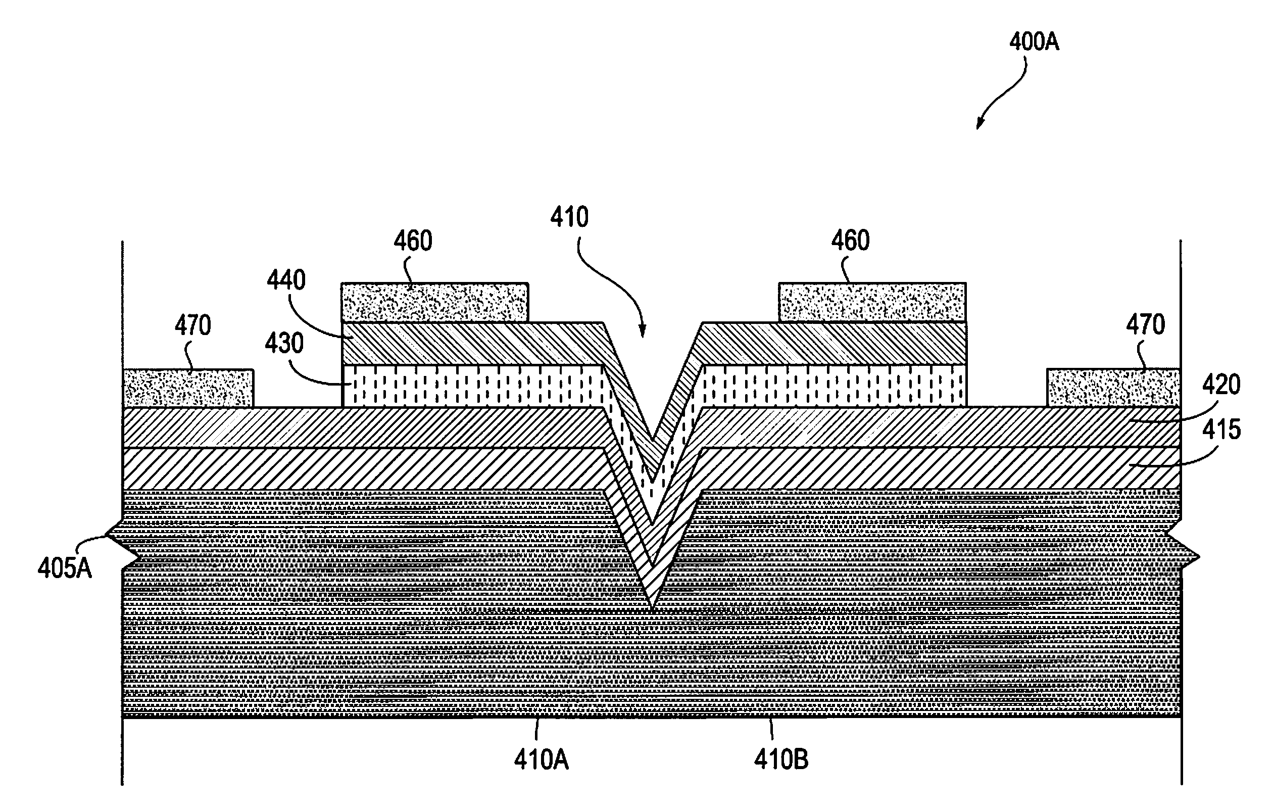
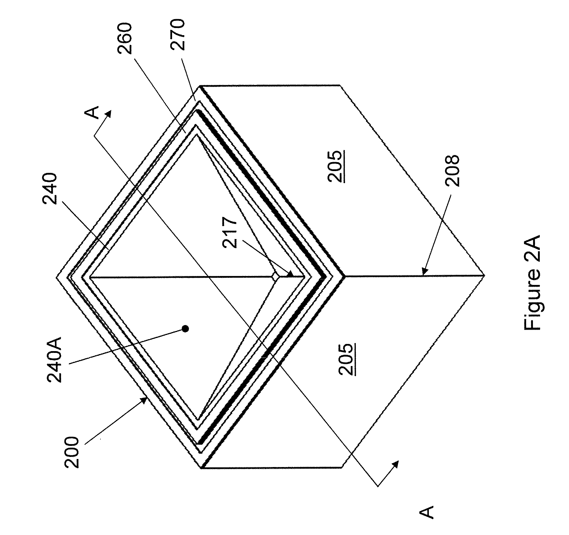
[0049]Referring to FIGS. 2A to 3C, a light emitting device 200 is formed on a substrate 205 having an upper surface 207 (FIG. 3B). The light emitting device 200 includes a trench 210 in the substrate 205 below the upper surface 207. The trench 210 has one or more trench surfaces 213 (FIG. 3B) at a slope relative to the upper surface 207. The trench 210 can also have a bottom surface 219 that is parallel to the upper surface 207. The area of the bottom surface 219 can be kept smaller than 20% of one of the trench surfaces 213. The substrate 205 can be silicon based: the upper surface 207 can be parallel to the (100) crystalline plane. The trench surface 213 can be parallel to the (111) crystalline surface. (Alternatively, the upper surface 207 can be parallel to the (111) crystalline plane. The trench surface 213 can be parallel to the (100) crystalline surface.) The trench 210 thus can have the shape of an inverted pyramid or a truncated inverted pyramid in the substrate 205, which ...


PUM


Abstract

A light emitting device includes a substrate having a first surface and a second surface not parallel to the first surface, and a light emission layer disposed over the second surface to emit light. The light emission layer has a light emission surface which is not parallel to the first surface.

Description

[0001]This application is a continuation-in-part of U.S. patent application Ser. No. 11 / 761,446 of S. Pan, filed on Jun. 12, 2007, which is incorporated herein by reference.BACKGROUND[0002]The present patent application is related to light emitting devices.[0003]Solid-state light sources, such as light emitting diodes (LEDs) and laser diodes, can offer significant advantages over other forms of lighting, such as incandescent or fluorescent lighting. For example, when LEDs or laser diodes are placed in arrays of red, green and blue elements, they can act as a source for white light or as a multi-colored display. In such configurations, solid-state light sources are generally more efficient and produce less heat than traditional incandescent or fluorescent lights. Although solid-state lighting offers certain advantages, conventional semiconductor structures and devices used for solid-state lighting are relatively expensive. One of the costs related to conventional solid-state light em...

Claims


Application Information

Patent Timeline
Patent Type & Authority Applications(United States)
IPC IPC(8): H01L33/00H01L33/10H01L33/20H01L33/24H01L33/32
CPCH01L33/10H01L33/32H01L33/24H01L33/20
Inventor PAN, SHAOHER X.
Owner SIPHOTON
Why Eureka
Try Eureka