
Microelectronic assembly having variable thickness solder joint

Inactive Publication Date: 2005-11-17
DELPHI TECH INC
View PDF10 Cites 2 Cited by
  • Summary
  • Abstract
  • Description
  • Claims
  • Application Information

AI Technical Summary

Benefits of technology

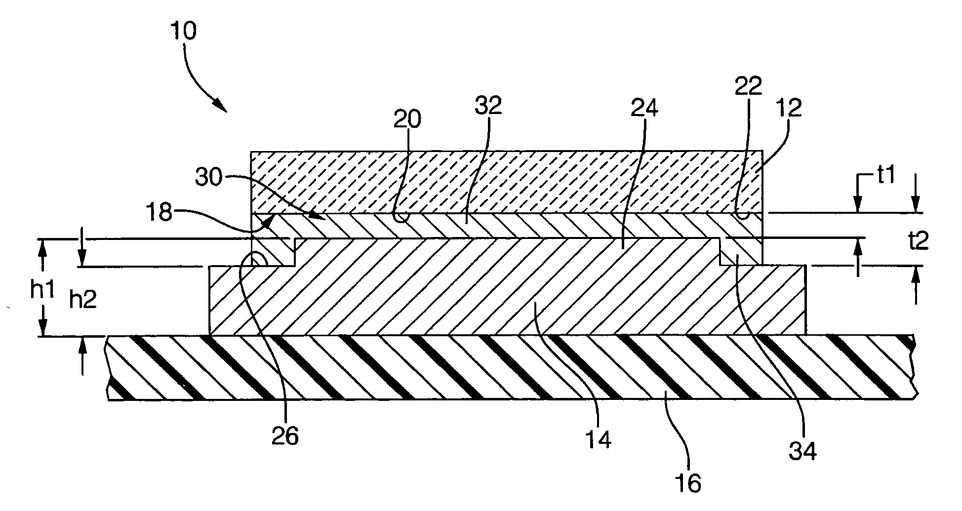
[0005] In accordance with this invention, a microelectronic assembly comprises a component, such as a power die, attached to a substrate by a solder layer. The component face includes a central region surrounded by a perimeter region. The solder layer is characterized by a first thickness underlying the central region, and a second thickness underlying the perimeter region that is greater than the first thickness. Thus, the solder layer is thinner in the central section, to promote heat transfer from the component to the substrate. Further, the solder layer is greater at the perimeter where stresses due to thermal expansion mismatch tend to accumulate, and so is better able to resist fatigue that might otherwise result in failure of the device.

Problems solved by technology

Because of the difference between the CTE of the silicon die and the CTE of the copper heat sink, stress occurs within the solder layer that causes fatigue of the solder metal and lead to cracking of the joint and failure of the assembly.
However, solder tends to exhibit a relatively low thermal conductivity compared to copper or other heat sink metals, so that thicker solder reduces heat transfer form the die and is less effective for purposes of maintaining the die within a desired operating temperature range.

Method used


Image

  • Microelectronic assembly having variable thickness solder joint
  • Microelectronic assembly having variable thickness solder joint

Examples


Embodiment Construction

[0009] In accordance with a preferred embodiment of this invention, referring to FIG. 1, a microelectronic assembly 10 comprises a surface mount component 12 attached to a substrate 14 carried on a printed circuit board 16. By way of a preferred example, component 12 is a power die formed of silicon, such as an FET or IGBT device, and is attached to a substrate that is formed of copper or other metal having a high heat capacity. During operation, heat generated by the component is transferred to and dissipated by the substrate, so that the substrate serves as a heat sink. In addition to serving as a heat sink, substrate 12 may have other uses, such as a bus bar. Optionally, assembly 10 may include an overmolded polymeric body encapsulating the component. While this invention is particularly useful for power die that generate high heat during operation, it may also be suitably employed with low power devices which, because of environmental or other reasons, requires enhanced thermal ...


PUM


Abstract

A microelectronic assembly includes a component attached to a substrate by a variable thickness solder joint. The solder joint comprises a first thickness adjacent the central region of the component and a second, relatively greater thickness adjacent the perimeter region of the component. The variable thickness solder joint may be used for attaching a power die to a metal heat sink on a printed circuit board, so that the relatively thin central portion promoted thermal dissipation to maintain the die within a desired operating temperature range, and the relatively thick perimeter region distributes thermally induced stresses to enhance joint strength and reduce fatigue cracking.

Description

TECHNICAL FIELD OF INVENTION [0001] This invention relates to a microelectronic assembly wherein a component is attached to a substrate by a solder layer, and more particularly, to such assembly wherein the solder layer is thinner at the central section of the component than at the perimeter. BACKGROUND OF INVENTION [0002] In a typical microelectronic assembly, heat generated by a power die or other component may be dissipated to a substrate to maintain the component within a desired operating temperature range. For example, a power die, such as a field effect transistor, referred to as an FET, or an insulated gate bipolar transistor device, referred to as an IGBT, may be attached to a heat sink on a printed circuit board. In another type of assembly, the power die may be attached to a tab and incorporated into an overmolded package that is subsequently clamped to a heat sink. The substrate to which the die is attached is preferably formed of a metal having high thermal conductivity...

Claims


Application Information

Patent Timeline
IPC IPC(8): H01L21/60H01L23/373H01L23/52H01L29/06H05K1/11H05K1/16H05K3/34
CPCH01L23/3735H01L24/32H01L2924/1305H01L2924/1306H01L2924/10253H01L2924/014H01L2924/01006H05K2201/10969H05K2201/10166H01L24/83H01L29/0657H01L2224/27013H01L2224/32014H01L2224/32057H01L2224/83051H01L2224/83385H01L2224/83801H01L2924/01029H01L2924/0105H01L2924/01082H01L2924/01322H01L2924/10158H01L2924/13055H05K1/111H05K3/341H05K2201/09736H05K2201/09845H01L2924/3512H01L2924/00H01L2924/15747Y02P70/50
Inventor RUNYON, RONNIE JOEBERNDT, JOANNA CHRISTINEOBERLIN, GARY E.
Owner DELPHI TECH INC
Learn More