

Microstructure comprising a surface which is functionalised through the localised deposit of a thin layer and production method thereof
a microstructure and functionalisation technology, applied in the field of microstructures, can solve the problems of difficult to tally with a microstructure specification, traditional techniques for encapsulating pressure sensors, and inapplicability to these microstructures
- Summary
- Abstract
- Description
- Claims
- Application Information
AI Technical Summary
Benefits of technology
Problems solved by technology
Method used
Image

Examples
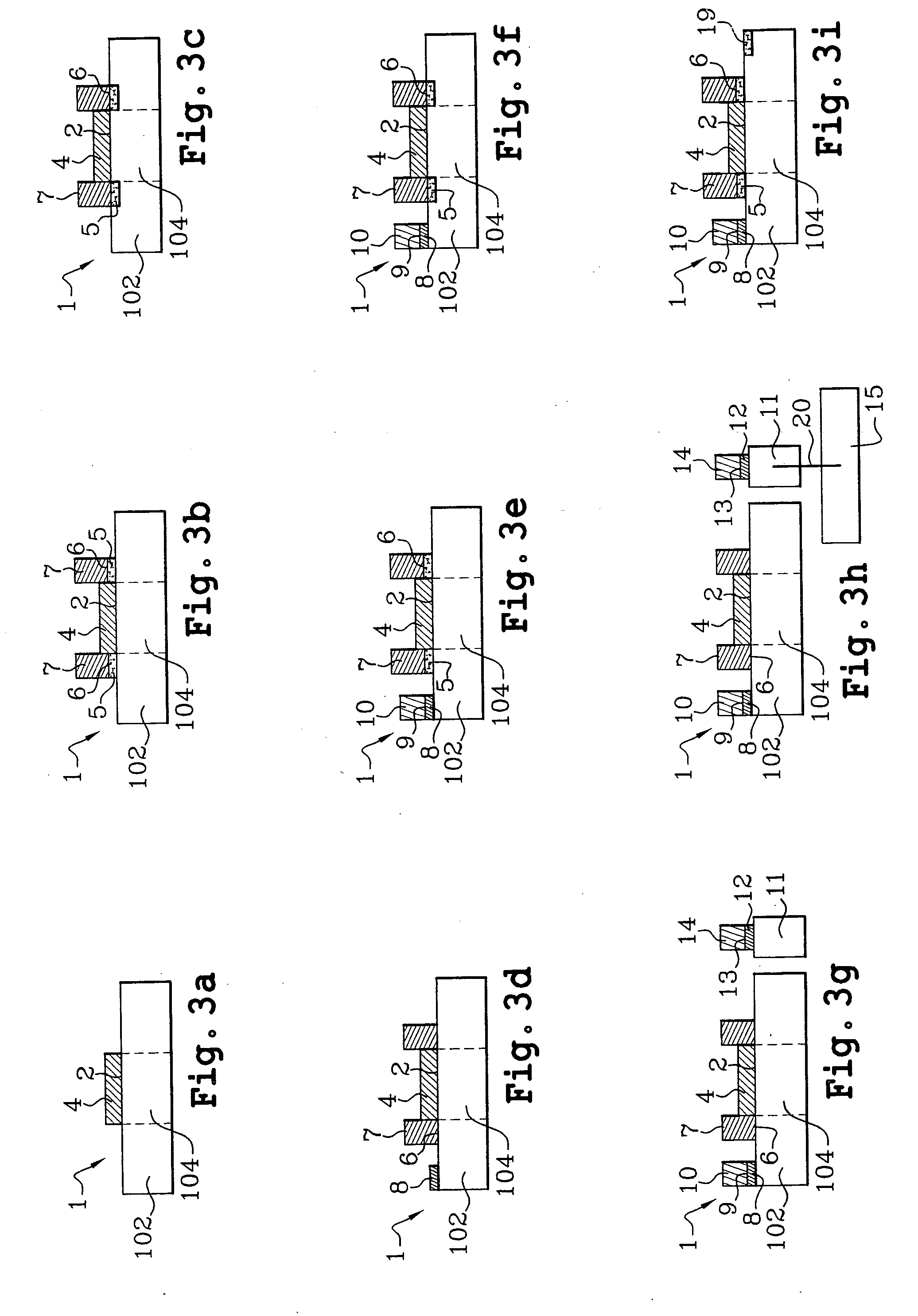
first embodiment
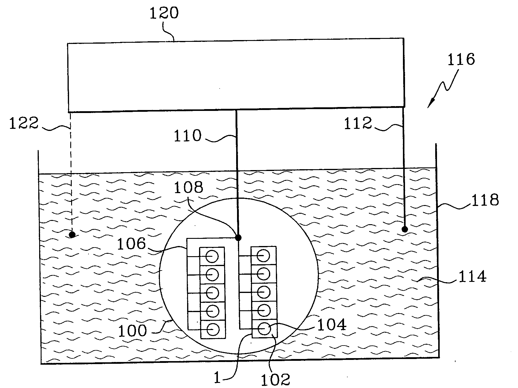
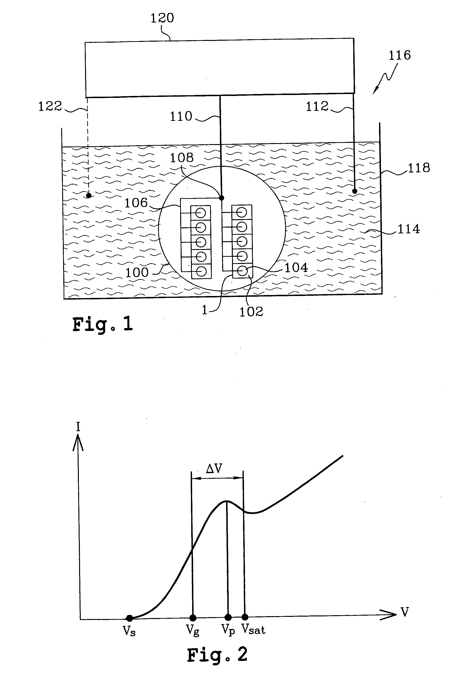
[0050] In a first embodiment, this wafer comprises a shared electrode different for each family, this electrode electrically connecting all of the pads belonging to this family of pads.
second embodiment
[0051] In a second embodiment, a same shared electrode is used for several families, each family being further characterised by a bare conductive surface (before its lining) of different chemical nature to the sense of the electrografting.
third embodiment
[0052] In a third embodiment, the shared electrode is connected to the different pads of a same family via impedances characterising a given family. Said impedances are diodes characterised by a conduction threshold, a zero conduction threshold being by convention attributed to a short circuit. A diode may be used to connect the shared electrode to one or several pads.
[0053] The diodes are oriented in such a way as to allow the flow of the electrochemical current during the formation of an organic film on the pads of the family considered. The diode is formed in such a way that its leakage current before the threshold is less than the residual electrochemical current before the formation of the organic film. In a specific embodiment, each pad of a family is associated either with a unique diode, or in a one-to-one manner with a diode of each microstructure.
[0054] These embodiments, unique shared electrode, shared electrode for families characterised by the chemical nature of the su...
PUM
| Property | Measurement | Unit |
|---|---|---|
| sizes | aaaaa | aaaaa |
| thickness | aaaaa | aaaaa |
| thickness | aaaaa | aaaaa |
Abstract
Description
Claims
Application Information