Non-magnetic semiconductor spin transistor

a non-magnetic semiconductor and spin transistor technology, applied in the field of semiconductor device electronics, can solve the problems of short spin relaxation time, serious trade-off, and unsatisfactory design constraints of spin-based semiconductor devices, and achieve the effect of high sensitivity of long-lived spin states

Inactive Publication Date: 2005-12-01
UNIV OF IOWA RES FOUND
View PDF18 Cites 78 Cited by
  • Summary
  • Abstract
  • Description
  • Claims
  • Application Information

AI Technical Summary

Benefits of technology

[0012] The present invention encompasses a spin resonant tunnel diode (spin RTD) and a spin transistor that exploit the unique characteristics of a spin-orbit pseudomagnetic field (BIA field) due to bulk inversion asymmetry (BIA) in (110)-oriented heterostructures. These devices are constructed using nonmagnetic materials. The BIA field in (110)-oriented quantum wells has a single orientation for all electron momenta (approximately in the (110) growth direction

Problems solved by technology

Semiconductor spintronics has been identified as an emerging research direction for logic applications due to possible improvements in power consumption, which represents a fundamental limitation in scaling for silicon-based CMOS technologies beyond the next decade.
This pseudomagnetic field structure (which differs in cases (i) and (ii) above) may lead to severe, undesirable design constraints for spin-based semiconductor devices.
This causes a serious trade-off between the size of the Rashba field and the spin relaxation time.
Spin manipulation in a practical device requires a strong Rashba field, but a str

Method used


Image

  • Non-magnetic semiconductor spin transistor
  • Non-magnetic semiconductor spin transistor
  • Non-magnetic semiconductor spin transistor

Examples


Embodiment Construction

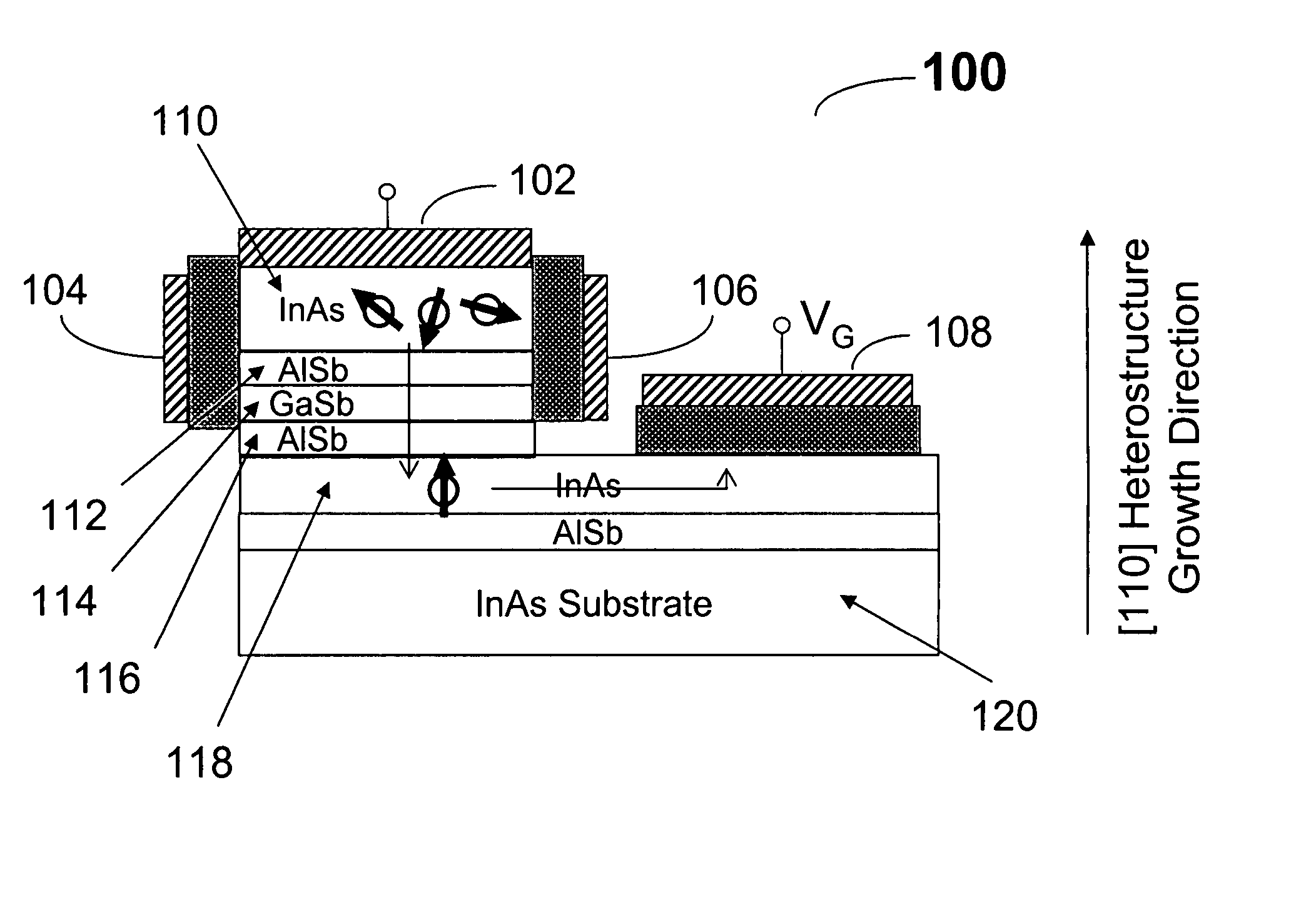
[0028] In the following detailed description, reference is made to the accompanying drawings, which form a part hereof, and in which is shown by way of illustration specific embodiments in which the invention may be practiced. These embodiments are described in sufficient detail to enable those skilled in the art to practice the invention, and it is to be understood that other embodiments may be utilized, and that structural, logical and programming changes may be made without departing from the spirit and scope of the present invention.

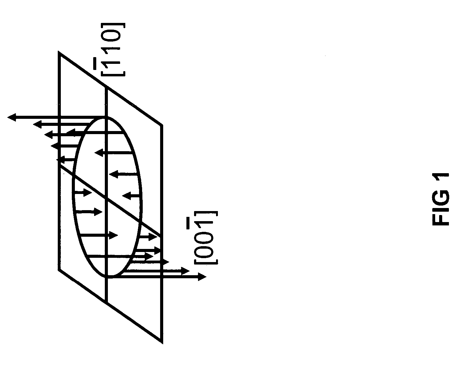
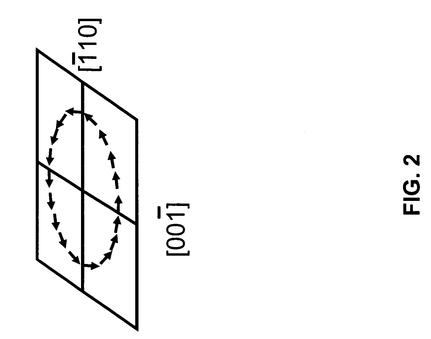
[0029] The present invention utilizes spin-related characteristics associated with (110)-oriented III-V semiconductor heterostructures. In a structurally-symmetric III-V semiconductor quantum well grown in the (110) orientation, a BIA field has a single orientation (nearly aligned with the (110) growth direction) which is independent of the momentum of the electron. A schematic representation of the BIA field in terms of the in-plane wavevector of t...


PUM


Abstract

A nonmagnetic semiconductor device which may be utilized as a spin resonant tunnel diode (spin RTD) and spin transistor, in which low applied voltages and/or magnetic fields are used to control the characteristics of spin-polarized current flow. The nonmagnetic semiconductor device exploits the properties of bulk inversion asymmetry (BIA) in (110)-oriented quantum wells. The nonmagnetic semiconductor device may also be used as a nonmagnetic semiconductor spin valve and a magnetic field sensor. The spin transistor and spin valve may be applied to low-power and/or high-density and/or high-speed logic technologies. The magnetic field sensor may be applied to high-speed hard disk read heads. The spin RTD of the present invention would be useful for a plurality of semiconductor spintronic devices for spin injection and/or spin detection.

Description

CROSS-REFERENCE TO RELATED APPLICATION [0001] This application claims priority to, and incorporates by reference, U.S. Application No. 60 / 548,395 entitled “Nonmagnetic Semiconductor Spin Transistor” filed on Feb. 27, 2004.STATEMENT REGARDING FEDERALLY SPONSORED RESEARCH OR DEVELOPMENT [0002] The U.S. Government has a paid-up license in this invention and the right in limited circumstances to require the patent owner to license others on reasonable terms as provided for by the terms of Grant No. DARPA MDA972-01-C-0002 and DARPA / ARO DAAD19-01-1-0490 awarded by The Defense Advanced Research Projects Agency.BACKGROUND OF THE INVENTION [0003] 1. Field of the Invention [0004] The present invention relates to semiconductor device electronics in the areas of semiconductor-based logic, magnetoresistive devices, and magnetic sensor technology. The present invention includes a spin resonant tunnel diode and spin transistor that operate by controlling spin-polarized current flow using low appli...

Claims


Application Information

Patent Timeline
IPC IPC(8): H01L29/06H01L29/66
CPCH01L29/66984B82Y10/00Y10S977/935
Inventor HALL, KIMBERLEY C.LAU, WAYNE H.GUNDOGDU, KENANFLATTE, MICHAEL E.BOGGESS, THOMAS F.
Owner UNIV OF IOWA RES FOUND
Why Eureka
Try Eureka