Multiple-gate MOS transistor and a method of manufacturing the same

Inactive Publication Date: 2005-12-01
III HLDG 2
View PDF5 Cites 81 Cited by
  • Summary
  • Abstract
  • Description
  • Claims
  • Application Information

AI Technical Summary

Benefits of technology

[0014] Therefore, in order to overcome the problems, the present invention is directed to a multiple-gate MOS transistor and method for manufacturing the same, capable of preventing degradation of reliability due to conce

Problems solved by technology

Second, when forming the fin having the single crystal silicon pattern as mentioned above, it is difficult to form the pattern to be thin and high and the fin of the channel region is formed in a rectangular shape.
For these reasons, there occur

Method used


Image

  • Multiple-gate MOS transistor and a method of manufacturing the same
  • Multiple-gate MOS transistor and a method of manufacturing the same
  • Multiple-gate MOS transistor and a method of manufacturing the same

Examples


Embodiment Construction

[0033] Hereinafter, the preferred embodiments of the present invention will be explained with reference to the accompanying drawings.

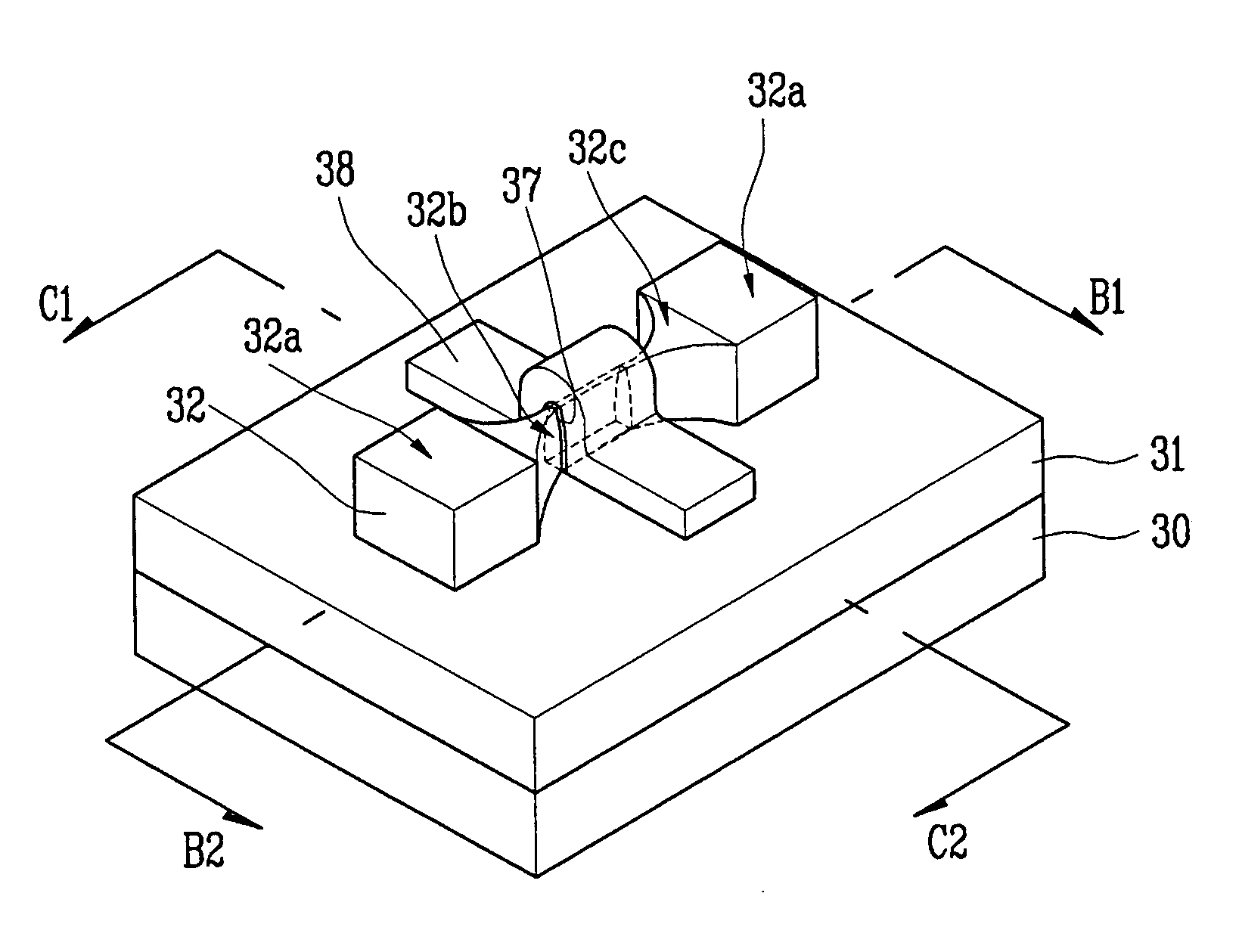
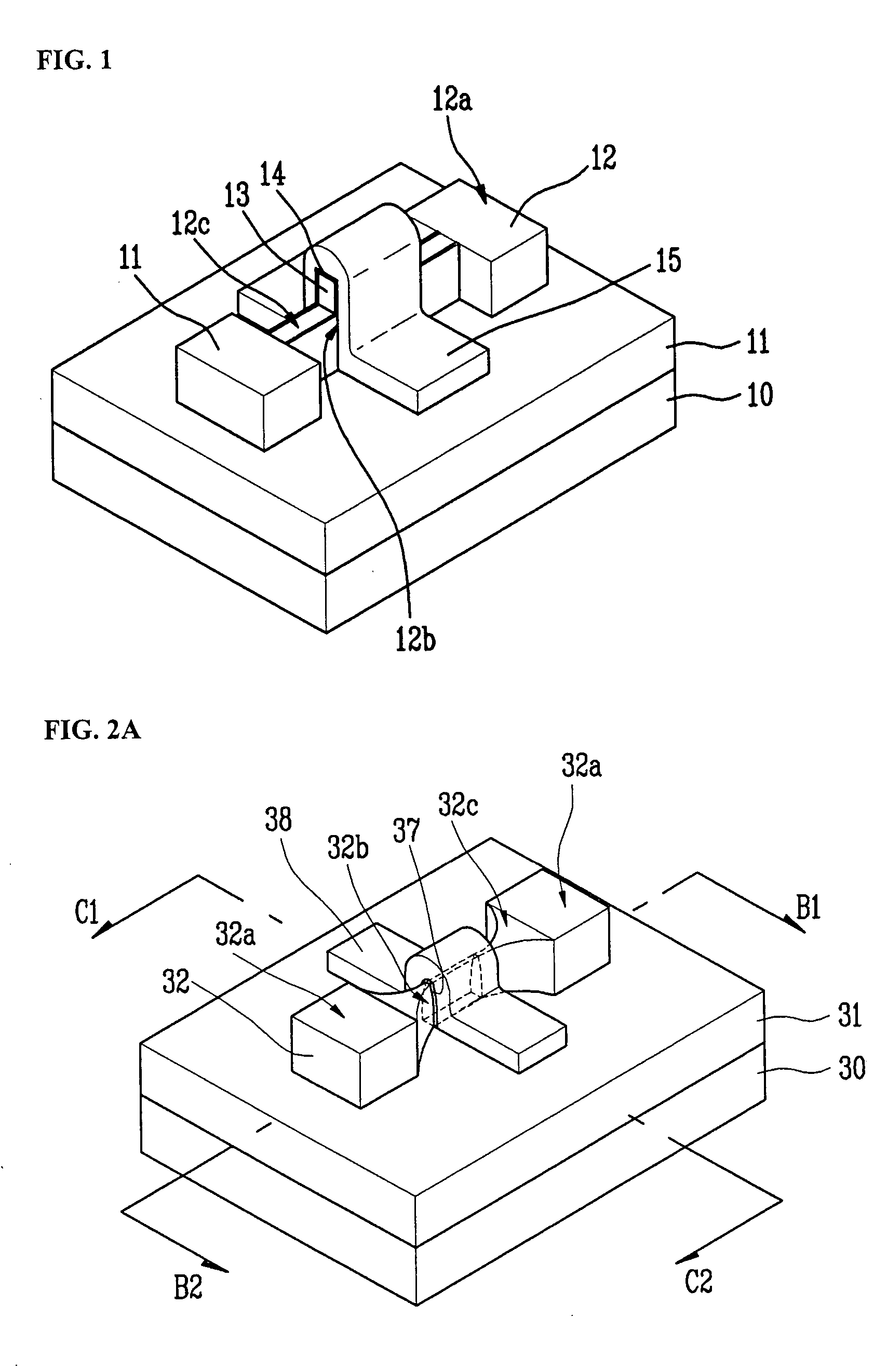
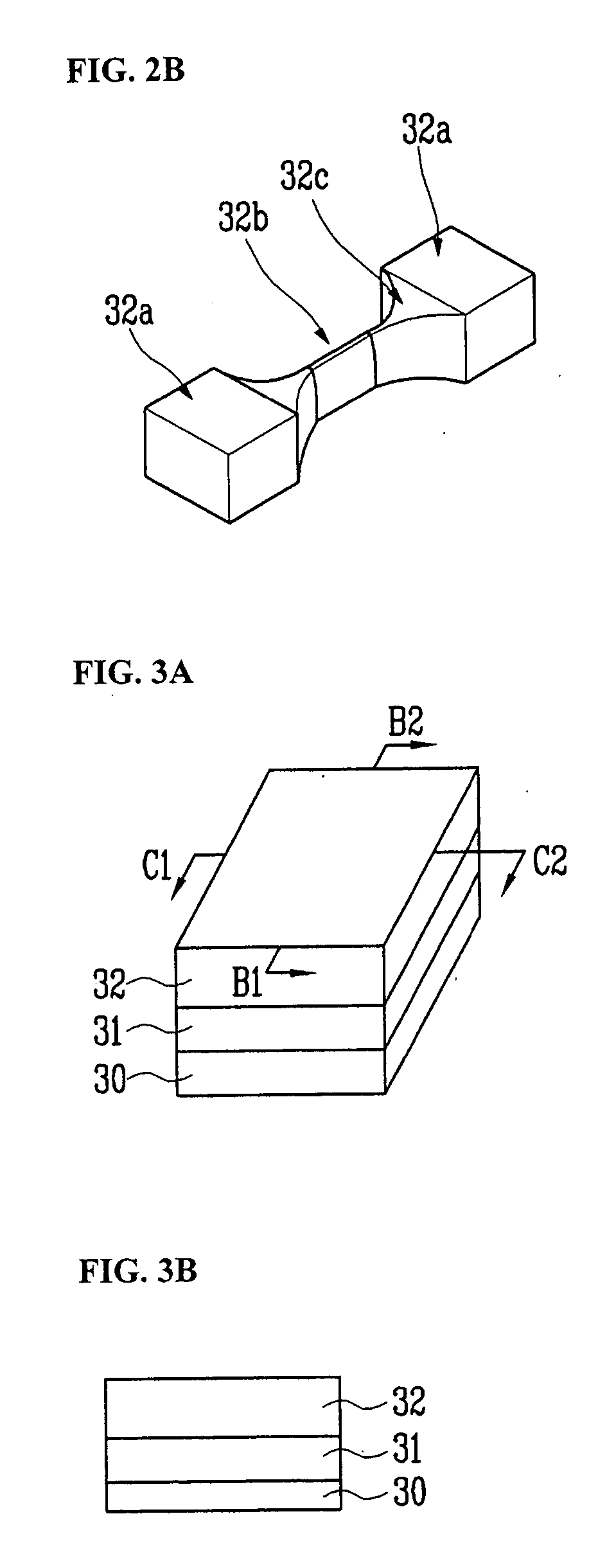
[0034]FIG. 2a is a perspective view for explaining a multiple-gate metal oxide semiconductor field effect transistor (MOSFET) according to one embodiment of the present invention, and FIG. 2b is a perspective view showing only the single-crystal silicon pattern of FIG. 2a.

[0035] A silicon on insulator (SOI) substrate is used, on which a silicon layer 30, an oxide layer 31, and a single-crystal layer 32 are laminated. The single-crystal silicon pattern 32 is formed by patterning the single-crystal silicon layer 32. The single-crystal silicon pattern 32 is allowed to define source and drain regions 32a, a channel region 32b formed between the source and drain regions 32a, and an extension region 32c interconnecting the source and drain regions 32a with the channel region 32b (see FIG. 2a).

[0036] The single-crystal silicon pattern 32 of the channel reg...


PUM


Abstract

Provided is a multiple-gate metal oxide semiconductor (MOS) transistor and a method for manufacturing the same, in which a channel is implemented in a streamline shape, an expansion region is implemented in a gradually increased form, and source and drain regions is implemented in an elevated structure by using a difference of a thermal oxidation rate depending on a crystal orientation of silicon and a geographical shape of the single-crystal silicon pattern. As the channel is formed in a streamline shape, it is possible to prevent the degradation of reliability due to concentration of an electric field and current driving capability by the gate voltage is improved because the upper portion and both sides of the channel are surrounded by the gate electrodes. In addition, a current crowding effect is prevented due to the expansion region increased in size and source and drain series resistance is reduced by elevated source and drain structures, thereby increasing the current driving capability.

Description

BACKGROUND [0001] 1. Field of the Invention [0002] The present invention relates generally to a multiple-gate metal oxide semiconductor (MOS) transistor and a method of manufacturing the same, and more particularly to a multiple-gate MOS transistor having a channel in a form of a streamline (∩), and a source and a drain in which a series resistance is reduced, and a method of manufacturing the same. [0003] 2. Discussion of Related Art [0004] As technology for manufacturing a semiconductor device is developed, many efforts have been made to improve performance of the semiconductor device through a decrease in size, an increase in operating speed, and so on. Hence, in the case of a metal-oxide-semiconductor field-effect transistor (MOSFET) which has constituted the principal axis of devices used in the electronic field today, the size decrease (scale down) has been continued. However, when a length of a channel decreases to 100 nm or less, the MOSFET is generally lowered in ON / OFF con...

Claims


Application Information

Patent Timeline
IPC IPC(8): H01L21/336H01L27/12H01L29/786
CPCH01L29/785H01L29/66818B24B7/22B24B27/0061B24B47/04B24B47/14B24B7/04
Inventor CHO, YOUNG KYUNKWON, SUNG KUROH, TAE MOONLEE, DAE WOOKIM, JONG DAE
Owner III HLDG 2
Why Eureka
Try Eureka