Multilayer printed wiring board and multilayer printed circuit board

a printed wiring board and multi-layer technology, applied in the direction of printed circuits, printed circuit stress/warp reduction, high frequency circuit adaptations, etc., can solve the problems of large stress applied to the solder ball, the disconnecting of the joint between the semiconductor device and the printed wiring board, and the cracking of the solder ball. , to achieve the effect of stabilizing the impedance of the wiring and reducing the stress of the solder joint portion

Inactive Publication Date: 2005-12-01
CANON KK
View PDF2 Cites 20 Cited by
  • Summary
  • Abstract
  • Description
  • Claims
  • Application Information

AI Technical Summary

Benefits of technology

[0011] It is an object of the present invention to provide a multilayer printed wiring board capable of reducing the stress of the solder joint portion with a semiconductor device generated due to thermal expansion and stabilizing the impedance of a wiring.

Problems solved by technology

Because of the difference between the coefficients of thermal expansion, the printed wiring board greatly warps and thereby, a large stress is applied to a solder ball.
Therefore, a crack occurs on the solder ball or the joint between the semiconductor device and the printed wiring board is disconnected.
Therefore, how to maintain a joint strength by small solder ball is a large problem.
However, when the size of the continuous pattern of circle or polygon such as a hexagon is decreased, the coefficient of thermal expansion of a printed wiring board increases and the above problem of warp is actualized.

Method used


Image

  • Multilayer printed wiring board and multilayer printed circuit board
  • Multilayer printed wiring board and multilayer printed circuit board
  • Multilayer printed wiring board and multilayer printed circuit board

Examples


embodiment 1

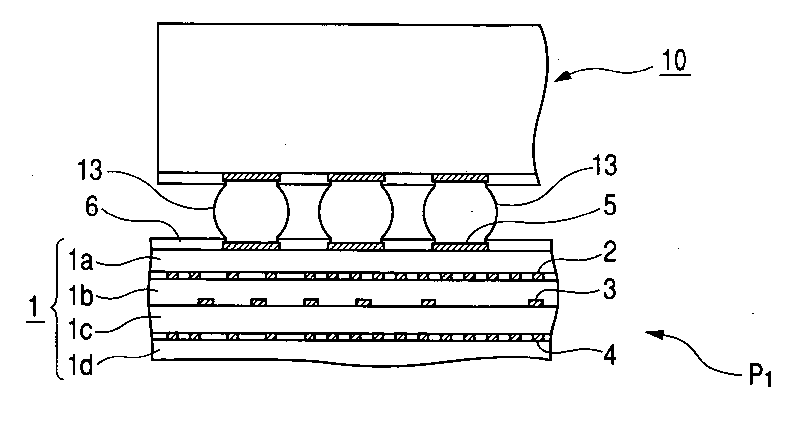
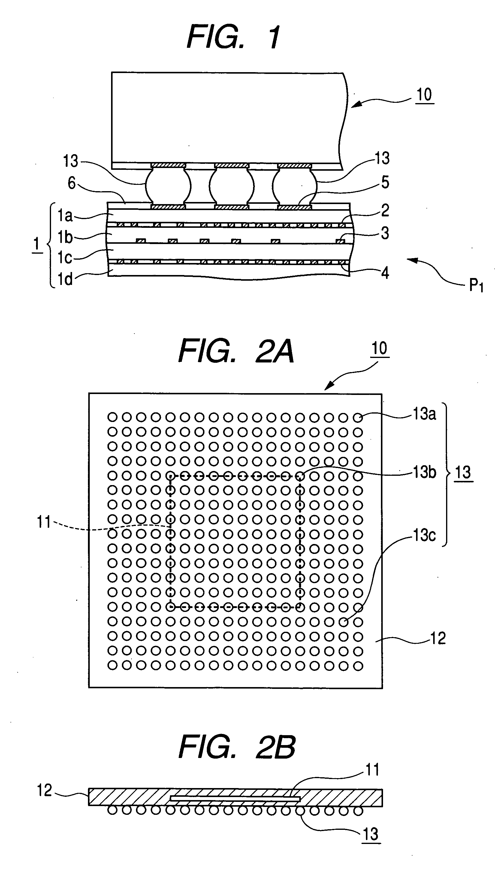
[0024]FIG. 1 is a sectional view of a multilayer printed wiring board of the Embodiment 1. In FIG. 1, a multilayer printed wiring board P1 is formed of laminated four resin layers 1a, 1b, 1c, and 1d. A first wiring pattern 2 is formed on the interfacial surface between the first resin layer 1a and the second resin layer 1b, a second wiring pattern 3 is formed on the interfacial surface between the second resin layer 1b and the third resin layer 1c, and a third wiring pattern 4 is formed on the interfacial surface between the third resin layer 1c and the fourth resin layer 1d. The first wiring pattern 2 is a ground layer, the second wiring pattern 3 is a signal wiring layer, and the third wiring pattern 4 is a power supply layer. The resin layers 1a, 1b, 1c, and 1d are respectively formed of a glass epoxy resin obtained by reinforcing an epoxy resin with glass cloth.

[0025] Moreover, a plurality of lands 5 are formed on the surface of the first resin layer 1a in the form of an array ...

embodiment 2

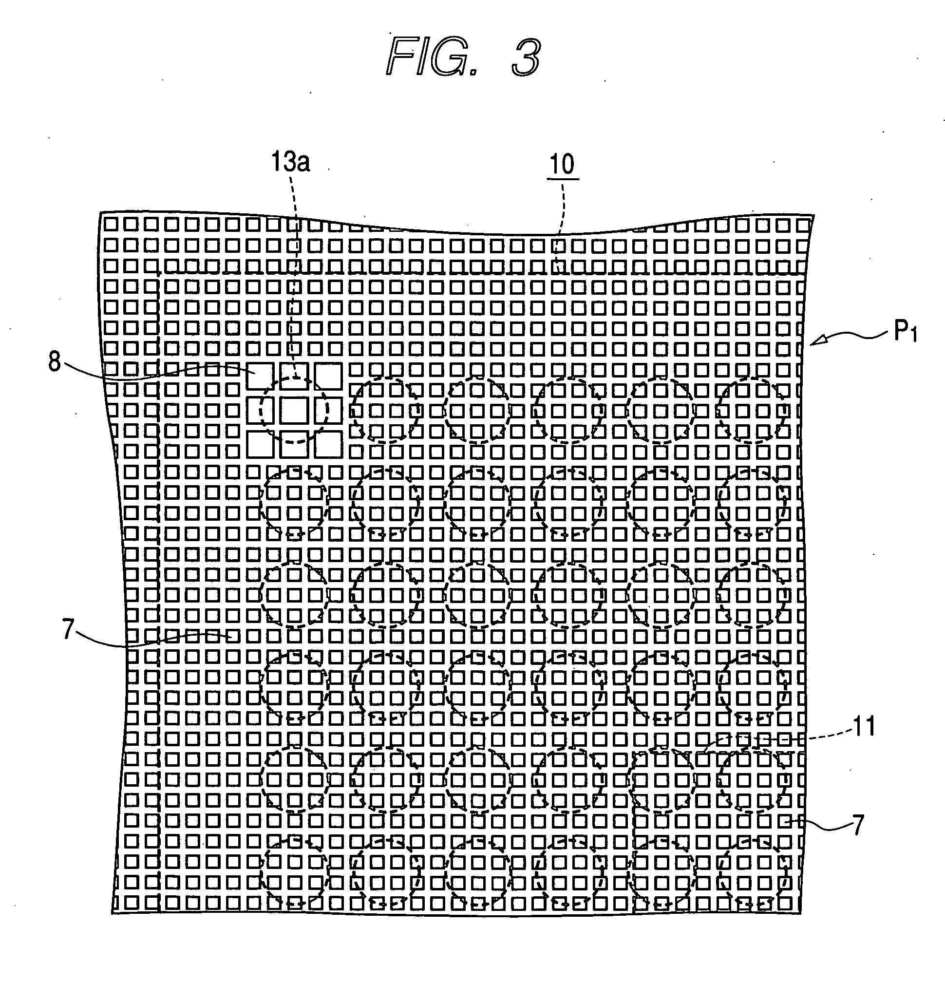
[0033]FIG. 4 is a top view showing a first wiring pattern 2 of a multilayer printed wiring board P2 of the Embodiment 2. To simplify the description, the contour of a semiconductor device 10, contour of an IC chip 11, and position of a solder ball 13 are shown by a dotted line. Rectangular openings are formed on the first wiring pattern 2 in the form of a mesh.

[0034] In FIG. 4, a joint portion where a maximum stress due to thermal expansion is generated is a solder ball 13a located at four corners of the solder balls arranged in the form of an array on the semiconductor device 10 shown in FIG. 3 as well as a solder ball 13b located at four corners of the IC chip 11. This is because the thermal expansion coefficient of a semiconductor device is greatly influenced by the IC chip 11 made of silicon, so that a large joint stress is generated also in the solder ball 13b located at four corners of the IC chip 11. In the first wiring pattern 2, a region corresponding to joint portions for...

embodiment 3

[0036]FIG. 5 is a top view showing a first wiring pattern 2 of a multilayer printed wiring board P3 of the Embodiment 3. To simplify the description, the contour of a semiconductor device 10, contour of an IC chip 11, and positions of solder balls 13a are shown by a dotted line. Rectangular openings are formed on the first wiring pattern 2 in the form of a mesh.

[0037] In FIG. 5, a portion at which a joint portion to generate a maximum stress due to thermal expansion is formed is a solder ball located at four corners of the semiconductor device 10 similarly to FIG. 3. In FIG. 5, in the first wiring pattern 2, a mesh opening 8 formed by a plurality of rectangular openings 9a is formed only on a portion corresponding to solder balls located at four corners of the semiconductor device 10. The other regions are constituted of a solid ground pattern 9b.

[0038] Thereby, a stress due to thermal expansion is reduced. Moreover, by forming the rectangular opening 9a into a fine mesh pitch, it...


PUM


Abstract

In a multilayer printed wiring board having a plurality of laminated resin layers, a plurality of wiring patterns formed on the interfacial surface of the resin layers, and a plurality of lands formed on the outermost layer of the resin layers and on which the solder is provided, at least one of the wiring patterns has a plurality of openings in the form of a mesh, the size of openings of the wiring patterns in a region corresponding to the position of solder in which a stress generated in the solder provided on the lands becomes a value larger than a desired value due to thermal deformation of the semiconductor device and the multilayer printed wiring board is larger than that of openings in the other regions.

Description

BACKGROUND OF THE INVENTION [0001] 1. Field of the Invention [0002] The present invention relates to a wiring pattern of a multilayer printed wiring board mounting a semiconductor device. [0003] 2. Related Background Art [0004] A printed circuit board in which a semiconductor device is mounted on a printed wiring board has been used so far for various products. Because wirings of a printed wiring board are increased in density, the BGA method and the CSP method for connecting a semiconductor device with a printed wiring board by a plurality of solder balls arranged like an array have been frequently used. Moreover, a multilayer printed wring board is generally used. [0005] It is requested for a solder ball for connecting a semiconductor device with a printed wiring board to keep a desired joint strength. To keep the joint strength, it is necessary to minimize a relative deformation between the printed wiring board and the semiconductor device. [0006] However, the printed wiring boar...

Claims


Application Information

Patent Timeline
Patent Type & Authority Applications(United States)
IPC IPC(8): H01L23/053H01L23/498H05K1/00H05K1/02H05K1/11
CPCH01L23/49816H01L23/49838H01L2924/15311H01L2924/3011H05K1/0224H01L2224/16225H05K1/0271H05K1/0298H05K1/111H05K2201/093H05K2201/09681H05K1/0253
Inventor SAWADA, YASUHIRO
Owner CANON KK
Why Eureka
Try Eureka