Discharge electrode and discharge lamp

a discharge lamp and discharge electrode technology, applied in the manufacture of discharge tube/lamps, discharge tube main electrodes, electrode systems, etc., can solve the problems of not always showing sufficient improvement in efficiency, the majority of supplied electric power is consumed, and the relative less efficiency of thermal types, etc., to achieve high efficiency secondary-electron emission and long life

Inactive Publication Date: 2005-12-01
KK TOSHIBA
View PDF5 Cites 22 Cited by
  • Summary
  • Abstract
  • Description
  • Claims
  • Application Information

AI Technical Summary

Benefits of technology

[0010] In view of these situations, it is an object of the present invention to provide a discharge electrode utilizing an electron-emitting layer facilitating a highly efficient secondary-electron emission and a longer lifetime, and various discharge lamps utilizing the discharge electrode.

Problems solved by technology

There is particularly a strong market demand for cold-cathode discharge lamps for backlights and the like as they are relatively less efficient than thermal types.
Hei 10-69868 and Japanese Patent Application Laid-open No. 2000-106130, most of the supplied electric power is consumed by the cathode material, not always showing sufficient improvement in efficiency.
However, there are problems of attributing to electric discharge from discharge lamps and wear-out of electrodes through sputtering due to Ar ion bombardment, resulting in a short lifetime without being able to maintain high efficiency over a long period of time.

Method used


Image

  • Discharge electrode and discharge lamp
  • Discharge electrode and discharge lamp
  • Discharge electrode and discharge lamp

Examples


first embodiment

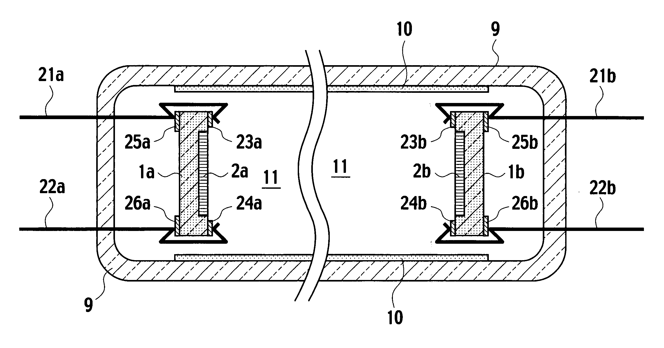
[0040] As shown in FIG. 1, a discharge lamp according to a first embodiment of the present invention encompasses a sealed-off tube 9 filled with a discharge gas 11, a fluorescent film 10, which is coated with a thickness of 50 μm to 300 μm to part of the inner wall of the sealed-off tube 9, and a pair of discharge electrodes (2a, 1a, 11a, 12a; 2b, 1b, 11b, 12b), which is provided in the inside of the sealed-off tube 9 at both sides. The sealed-off tube 9 may be a glass tube made of soda lime glass, boron silicate glass or the like, for example.

[0041] Of the pair of discharge electrodes (2a, 1a, 11a, 12a; 2b, 1b, 11b, 12b), a first discharge electrode (2a, 1a, 11a, 12a) on the left side of FIG. 1 encompasses a wide bandgap semiconductor substrate 1a as a “supporting base”, an electron-emitting layer 2a formed as an emitter at the top surface of the wide bandgap semiconductor substrate (supporting base) 1a, a bottom electrode 11a formed on the bottom surface of the wide bandgap semic...

second embodiment

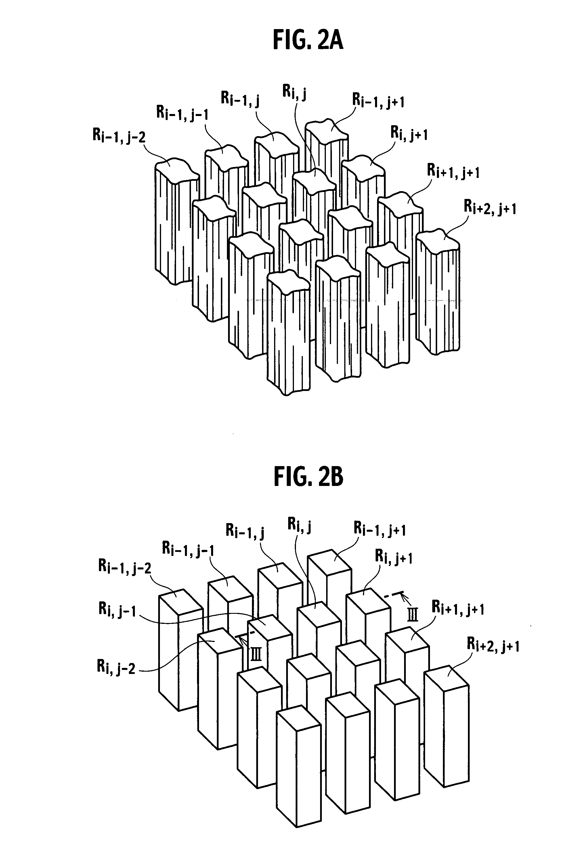
[0075]FIG. 9 is a fragmentary bird's eye view illustrating part of an electron-emitting layer 2a provided in a first discharge electrode of a discharge lamp, according to a second embodiment of the present invention, in which a part corresponding to portion A of FIG. 1 is enlarged. In the first discharge electrode of the discharge lamp, according to the second embodiment, a cathode base plate implemented by a wide bandgap semiconductor substrate1 made of diamonds, for example, has a plurality of fine pores Hi−1,j, . . . , Hi,j, . . . , Hi+2,j, . . . , which have sidewalls (vertical sidewalls) roughly parallel to electric fields perpendicular to the primary surfaces of the first discharge electrode. Dangling bonds on the surfaces of respective sidewalls (vertical sidewalls) of the fine pores Hi−1,j, . . . , Hi,j, . . . , Hi+2,j, . . . are subjected to hydrogen-termination treatment. Since the rest of the configuration of the discharge lamp is effectively the same as that of the disch...

third embodiment

[0087]FIG. 12 is a fragmentary bird's eye view illustrating part of an electron-emitting layer 2a in a first discharge electrode of a discharge lamp, according to the third embodiment of the present invention, which may corresponds to portion A in FIG. 1. The electron-emitting layer 2a is formed of a wide bandgap semiconductor and provided on a supporting base 45. The electron-emitting layer 2a is implemented by a plurality of protrusions, at least part of the surface of each of the protrusions is unseen from a perpendicular direction to a top surface of the electron-emitting layer 2a above the top surface of the electron-emitting layer 2a. As shown in FIG. 12, the protrusions are implemented by a plurality of wide bandgap semiconductor grains 4, each having a diameter “d”, agglomerated on the supporting base 45. Bonds of hydrogen atoms 3 terminate the dangling bonds on surfaces of respective wide bandgap semiconductor grains 4.

[0088] Diameter “d” of the respective wide bandgap sem...


PUM


Abstract

A discharge lamp encompassing a sealed-off tube filled with a discharge gas and a discharge electrode provided in the sealed-off tube. The discharge electrode embraces a supporting base and an electron-emitting layer formed of a wide bandgap semiconductor and provided on the supporting base, implemented by a plurality of protrusions, at least part of surfaces of the protrusions are unseen from a perpendicular direction to thereof above a top surface of the electron-emitting layer, dangling bonds of the wide bandgap semiconductor at the surfaces are terminated with hydrogen atoms.

Description

CROSS REFERENCE TO RELATED APPLICATIONS AND INCORPORATION BY REFERENCE [0001] This application claims benefit of priority under 35 USC 119 based on Japanese Patent Application No. P2004-162102 filed May 31, 2004, the entire contents of which are incorporated by reference herein. BACKGROUND OF THE INVENTION [0002] 1. Field of the Invention [0003] The instant invention relates to a discharge electrode utilizing an electron-emitting layer, and a discharge lamp utilizing the discharge electrode. [0004] 2. Description of the Related Art [0005] Discharge lamps have been widely used as a general use light source, an industrial light source, and various integrative light sources. Above all, a low voltage discharge lamp such as a fluorescent lamp has a big market dominating approximately half of the illuminative light source market. With these discharge lamps including the fluorescent lamp that form a big market, recent demands for resource saving, reduction in environmental load and the lik...

Claims


Application Information

Patent Timeline
Patent Type & Authority Applications(United States)
IPC IPC(8): H01J1/00H01J1/05H01J1/14H01J61/06H01J1/308H01J61/067H01J61/073
CPCH01J1/308H01J61/0737H01J61/0677
Inventor SAKAI, TADASHIONO, TOMIOSAKUMA, NAOSHIYOSHIDA, HIROAKISUZUKI, MARIKO
Owner KK TOSHIBA
Why Eureka
Try Eureka