Method and apparatus for detecting defects

a defect detection and defect technology, applied in the direction of optically investigating flaws/contamination, semiconductor/solid-state device testing/measurement, instruments, etc., can solve the problems of difficult to distinguish fine-structure foreign particles or microdefects from fine-structured foreign particles, edge roughness of workpiece patterns, etc., to improve the sensitivity of defect detection, reduce the coherence of laser light, and simple configuration

Inactive Publication Date: 2005-12-01
HITACHI HIGH-TECH CORP
View PDF19 Cites 35 Cited by
  • Summary
  • Abstract
  • Description
  • Claims
  • Application Information

AI Technical Summary

Benefits of technology

[0009] The present invention is intended to provide a defect detection method and apparatus that uses a high-coherence laser as a light source and is adapted to improve defect detection sensitivity with a simple configuration by reducing the coherence of laser l

Problems solved by technology

If foreign particles stick to or pattern defects occur on the surfaces of these workpieces during the manufacture of LSI and liquid-crystal substrates, this will cause pattern defects in workmanship, such as improper electrical wiring insulation or shor

Method used


Image

  • Method and apparatus for detecting defects
  • Method and apparatus for detecting defects
  • Method and apparatus for detecting defects

Examples


first embodiment

[0050] A first embodiment of the present invention will be described with reference to FIGS. 1 to 8.

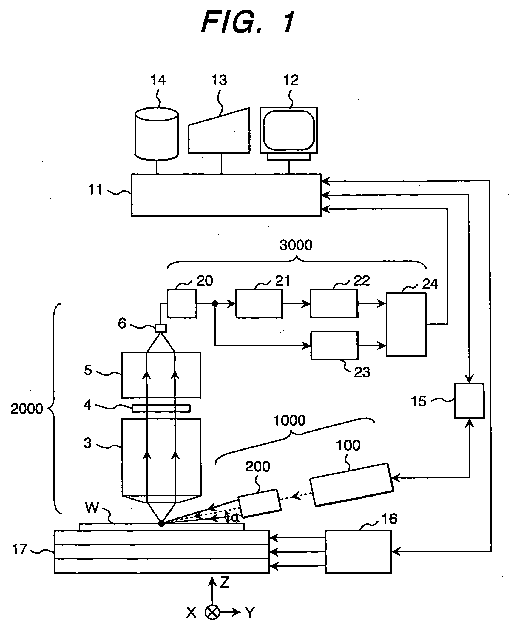
[0051] First, an example of a defect detection apparatus for detecting foreign particles and pattern defects on a semiconductor wafer is shown in FIG. 1. The defect detection apparatus is constructed so as to include: an irradiation optical system 1000, one feature of the present invention; a detection optical system 2000; an image processing unit 3000; a light source driver 15 that drives a laser light source 100; a main controller unit 11 that connects a display 12, an arithmetic device 13, a storage device 14, and an input / output section (network included) not shown, and controls the entire apparatus; an X-Y-Z stage 17 for resting thereon, for example, a semiconductor wafer W as an object to be subjected to defect detection, and moving the object W in X-, Y-, and Z-directions; and an X-Y-Z stage driver that conducts driving control of the X-Y-Z stage 17, based on commands from the...

second embodiment

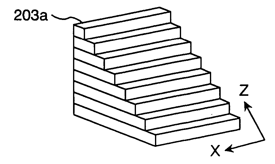
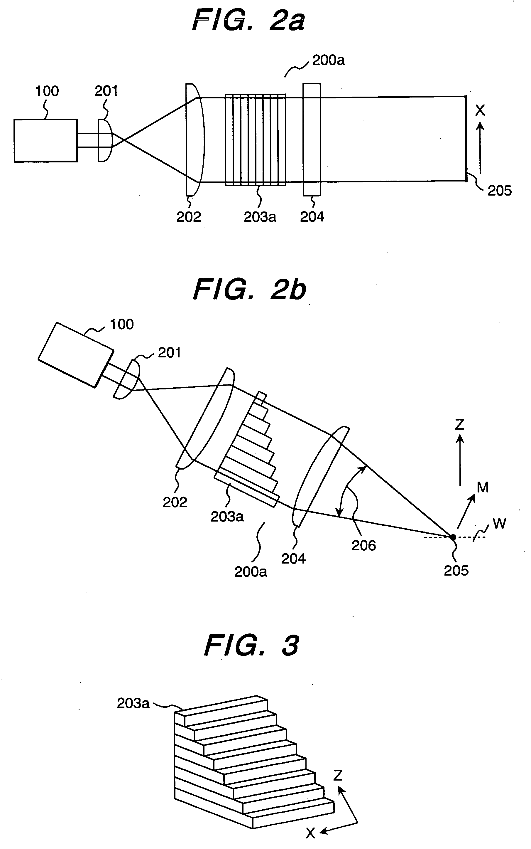
[0072] Next, a second embodiment of the present invention will be described using FIGS. 9 to 23a, 23b. The second embodiment differs from the first embodiment in that an irradiation system 200b in irradiation optical system 1000 uses a single-mode fiber bundle (single-mode fiber group) 300A whose optical path length is changed to reduce coherence.

[0073]FIG. 9 shows single-mode fiber bundle 300A which, when a high-coherence laser light source is used as a light source 100 to emit UV laser light or DUV laser light, maintains temporal (time-wise) coherence intact and reduces only spatial coherence. That is to say, single-mode fibers 300a of the single-mode fiber bundle 300A are each provided with an optical path length difference greater than a laser coherence length, and exit beams from the single-mode fibers 300a become mutually incoherent beams. Therefore, low-coherence light illumination using the laser that is the coherent light source becomes possible by irradiating an object W ...


PUM


Abstract

The present invention relates to a defect detection apparatus and method by which foreign particles and circuit pattern defects can be detected in distinction from the edge roughness of wiring on the substrate. The defect detection apparatus comprises an irradiation optical system includes: a beam expander; an optical member group formed by stacking multiple plate-like optical members each having a different optical path length at least in a beam-converging direction in order to admit the laser beam with the beam diameter extended by the beam expander and emit multiple slit-like beams each spatially reduced in coherence in the beam-converging direction; and beam-converging optical system by which the multiple slit-like beams each emitted from the optical member group is converged into a slit-like beam in the beam-converging direction and the slit-like beam is irradiated from an oblique direction onto the surface of the subject.

Description

BACKGROUND OF THE INVENTION [0001] The present invention relates to a method and apparatus for detecting any foreign particles or circuit pattern defects occurring during the manufacture of LSI and liquid-crystal substrates. [0002] Conventional technologies for detecting, in discrimination from the circuit patterns formed on semiconductor wafers, the foreign particles sticking to or defects present on the circuit patterns, are disclosed in Japanese Patent Laid-open Nos. 1-117024 (corresponding to U.S. Pat. No. 6,411,377), 8-210989, 2000-105203 (corresponding to U.S. Pat. No. 5,046,847), 2001-194323 (corresponding to U.S. Pat. No. 6,621,571), and 2003-177102 (corresponding to U.S. application Ser. No. 10 / 650,756). [0003] Japanese Patent Laid-open No. 1-117024 describes the technology intended for smoothing or averaging the intensity of the light reflected from the thin films formed on a substrate. In this case, first, laser light that has been emitted from a semiconductor oscillator ...

Claims


Application Information

Patent Timeline
IPC IPC(8): G01N21/88G01B11/30G01N21/89G01N21/94G01N21/95G01N21/956H01L21/66
CPCG01N21/8806G01N21/94G01N2021/9513G01N21/956G01N2021/8905G01N21/9501
Inventor NAKANO, HIROYUKINOGUCHI, MINORIOHSHIMA, YOSHIMASAUTO, SACHIOHAMAMATSU, AKIRAIWATA, HISAFUMIWATANABE, TETSUYAJINGU, TAKAHIROFUKUSHIMA, HIDEKI
Owner HITACHI HIGH-TECH CORP
Why Eureka
Try Eureka