
Techniques for operating semiconductor devices

Active Publication Date: 2005-12-01
IBM CORP
View PDF8 Cites 19 Cited by
  • Summary
  • Abstract
  • Description
  • Claims
  • Application Information

AI Technical Summary

Benefits of technology

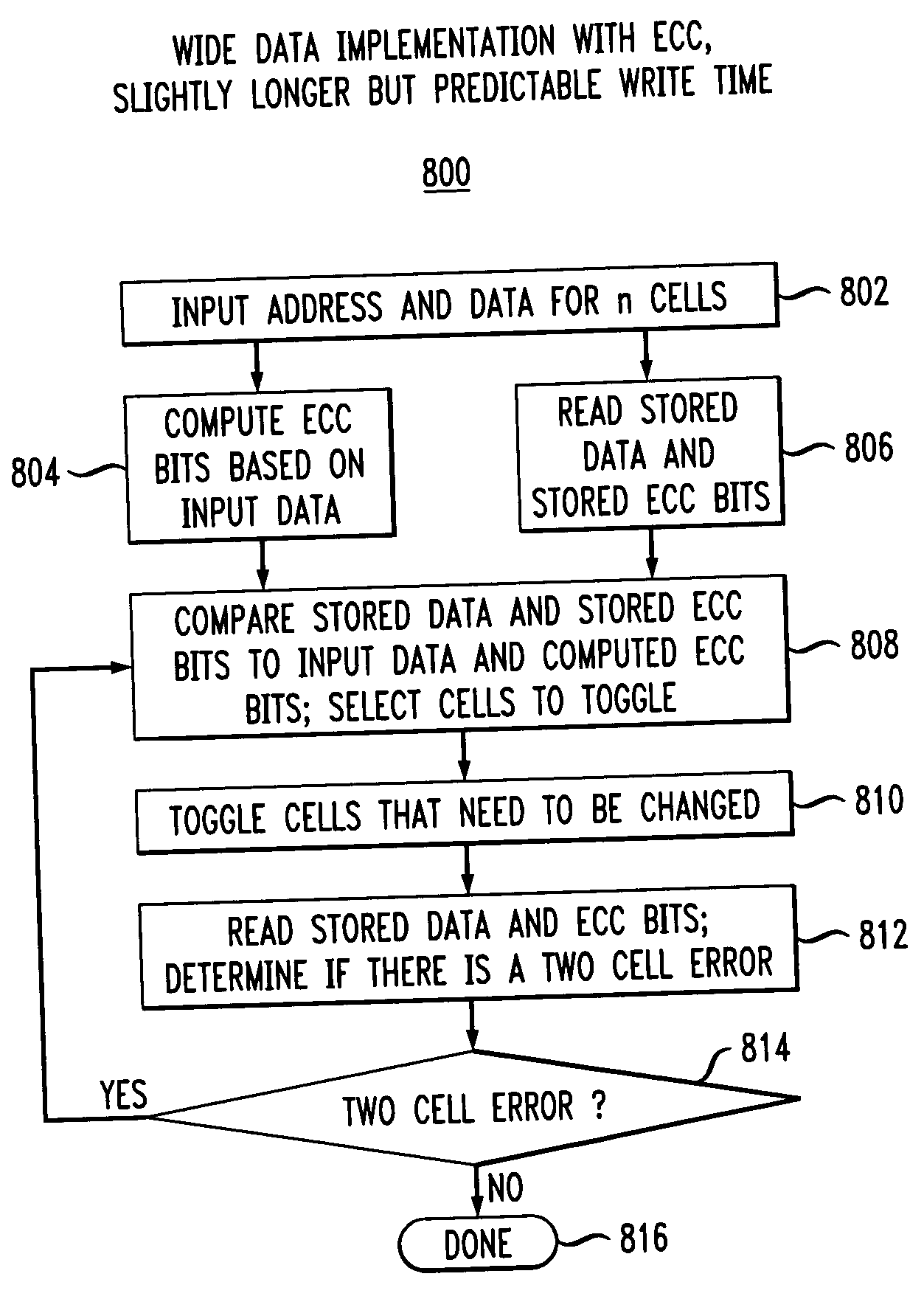
[0007] The present invention provides techniques for data storage. In one aspect of the invention, a method for writing one or more magnetic memory cells comprises the following steps. Data is written to one or more of the magnetic memo

Problems solved by technology

Unfortunately, in practice, the magnetization of one or more magnetic memory cells may change orientation unintentionally, due, at least in part, to thermal activation.
The resulting error rate due to thermally activated switching is called the soft error rate (SER).
However, lowering switching fields often undesirably lead to an increase in the SER.

Method used


Image

  • Techniques for operating semiconductor devices
  • Techniques for operating semiconductor devices
  • Techniques for operating semiconductor devices

Examples


Embodiment Construction

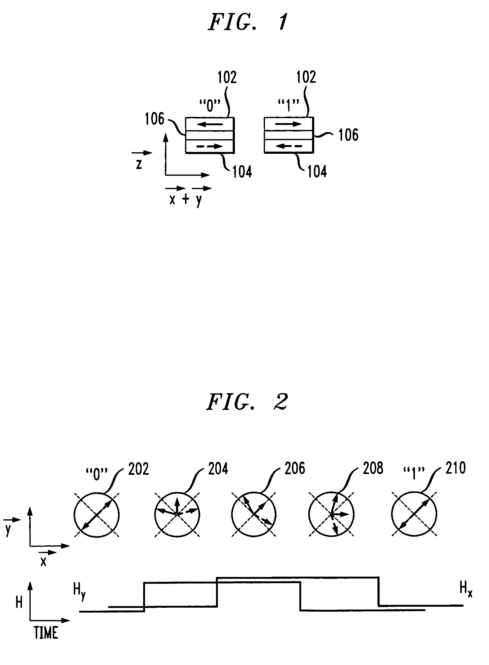
[0018]FIG. 1 is a diagram illustrating an exemplary free layer configuration of a magnetic memory cell having two anti-parallel coupled magnetic layers. Namely, in the exemplary configuration shown in FIG. 1, a free layer may comprise at least two magnetic layers, e.g., magnetic layers 102 and 104, anti-parallel coupled by spacer layer 106. Spacer layer 106 may comprise a transition metal. Suitable transition metals include, but are not limited to, chromium, copper, ruthenium, rhodium, palladium, rhenium, osmium, iridium, platinum and combinations comprising at least one of the foregoing transition metals.

[0019] A magnetic memory cell having a free layer comprising two anti-parallel coupled magnetic layers is hereinafter referred to as a “toggle magnetic memory cell.” U.S. Pat. No. 6,545,906 issued to Savtchenko et al. (hereinafter “Savtchenko”), the disclosure of which is incorporated by reference herein, discloses the use of such a toggle magnetic memory cell in an MRAM device. S...


PUM


Abstract

Techniques for data storage are provided. In one aspect, a method for writing one or more magnetic memory cells comprises the following steps. Data is written to one or more of the magnetic memory cells. It is detected whether there are any errors in the data written to the one or more magnetic memory cells. The data is rewritten to each of the one or more previously written magnetic memory cells in which an error is detected.

Description

FIELD OF THE INVENTION [0001] The present invention relates to semiconductor devices and, more particularly, to techniques for data storage in semiconductor devices. BACKGROUND OF THE INVENTION [0002] Certain semiconductor devices, e.g., magnetic random access memory (MRAM) devices, use magnetic memory cells to store information. Each magnetic memory cell typically comprises a submicron piece of magnetic material, e.g., having the dimensions of 300 nanometers (nm) by 600 nm in area and five nm thick. [0003] Information is stored in such semiconductor devices as an orientation of the magnetization of a free layer in the magnetic memory cell as compared to an orientation of the magnetization of a fixed (e.g., reference) layer in the memory cell. The magnetization of the free layer may be oriented parallel or anti-parallel relative to the fixed layer, representing either a logic “1” or a “0.” The orientation of the magnetization of a given layer (fixed or free) may be represented by an...

Claims


Application Information

Patent Timeline
IPC IPC(8): G11C11/15G11C11/16G11C29/00
CPCG11C11/16
Inventor GALLAGHER, WILLIAM JOSEPHWORLEDGE, DANIEL CHRISTOPHER
Owner IBM CORP
Learn More