

Ta sputtering target and method for preparation thereof
a sputtering target and target technology, applied in the field of ta sputtering targets, can solve the problems of deteriorating film quality, affecting the quality of sputtering deposition, and forming streaks from the center to the peripheral edge, and achieve the effect of stably manufacturing a ta sputtering target superior in characteristics
- Summary
- Abstract
- Description
- Claims
- Application Information
AI Technical Summary
Benefits of technology
Problems solved by technology
Method used
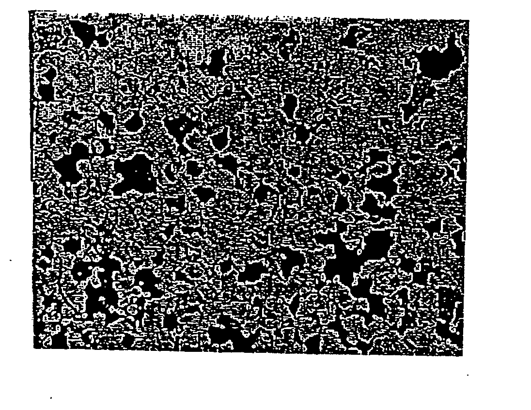
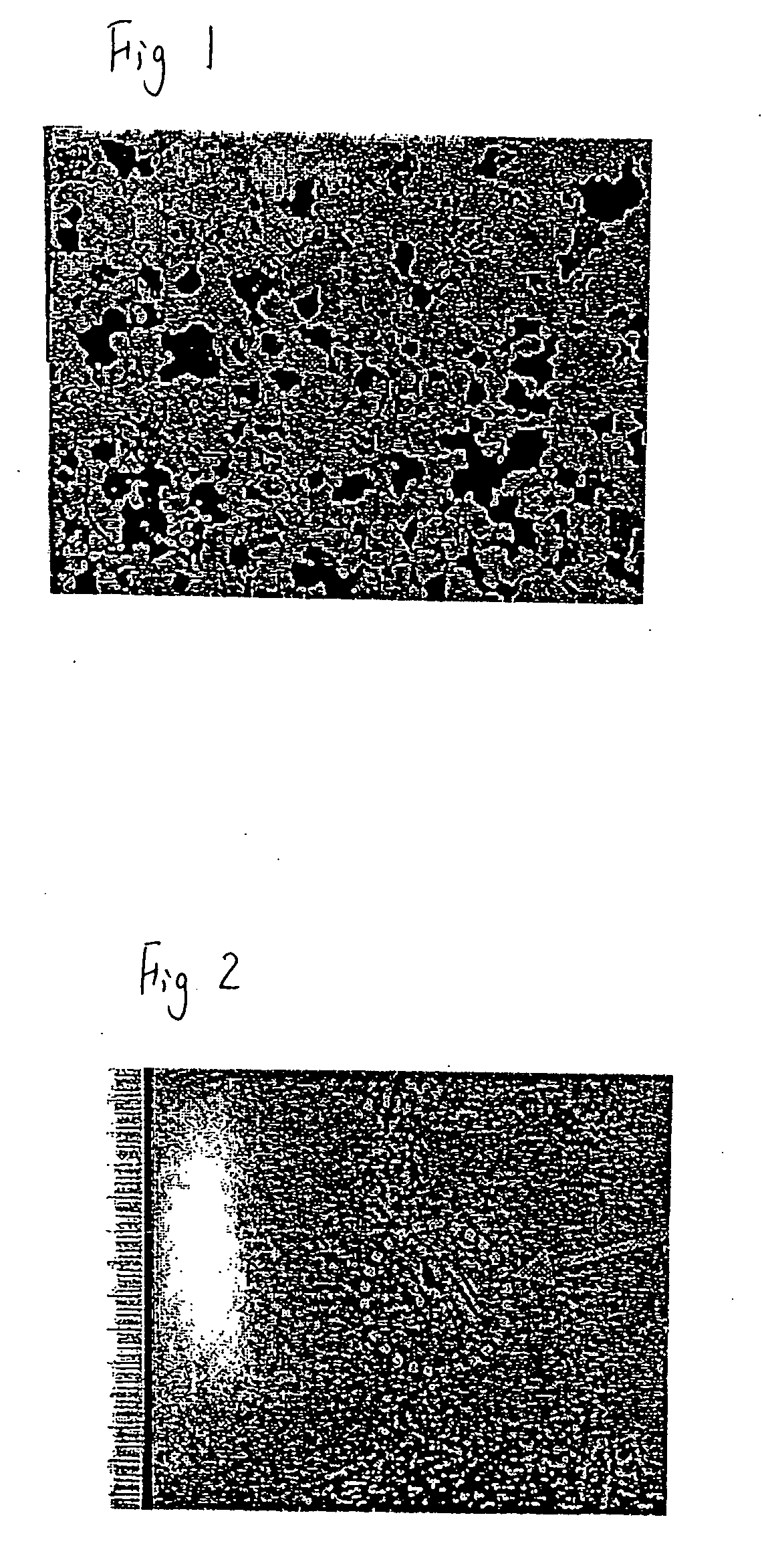
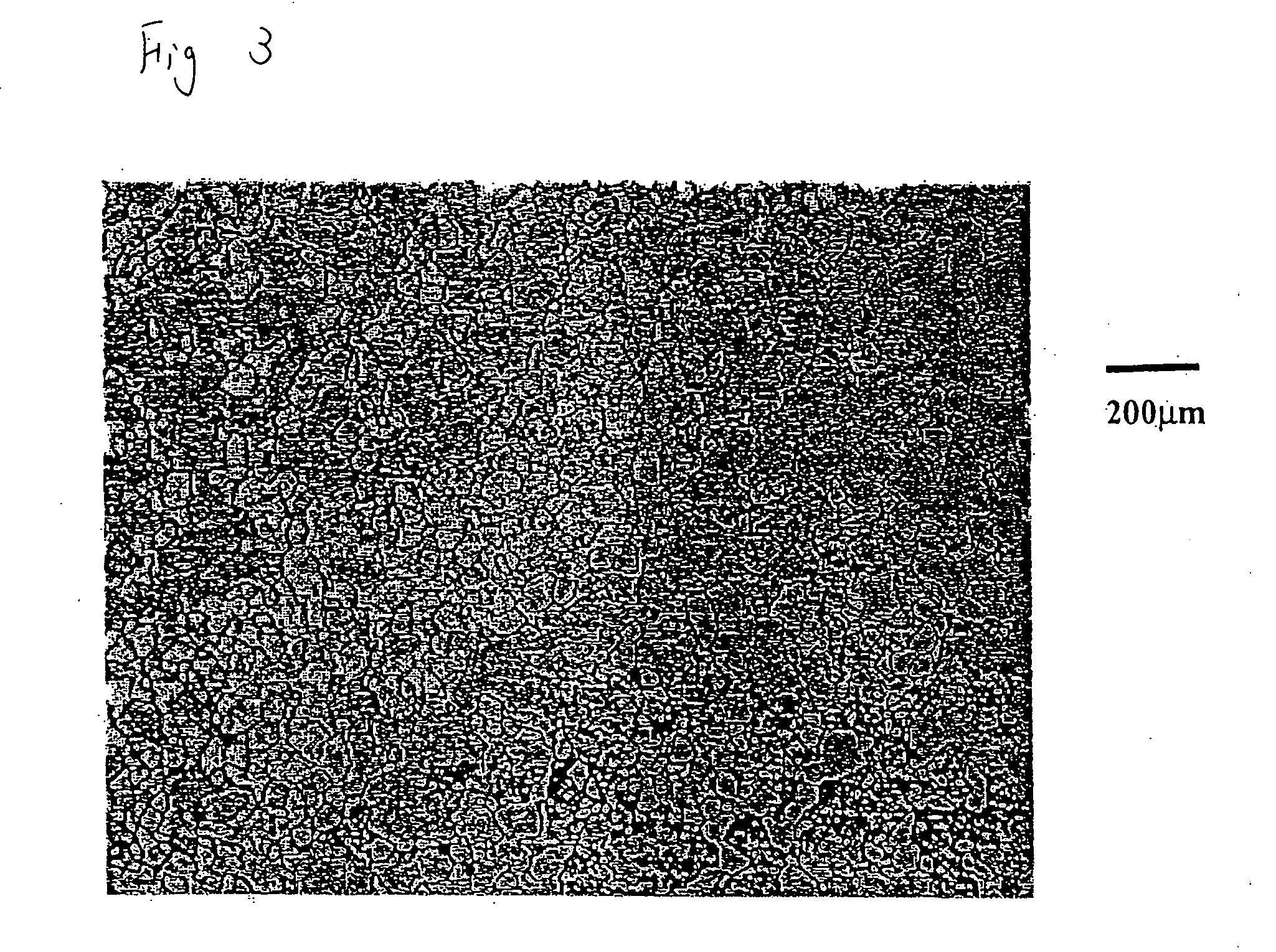
Image

Examples
example 1
[0040] A tantalum raw material having a purity of 99.997% was subject to electron beam melting, and this was cast to prepare an ingot or billet having a thickness of 200 mm and diameter of 200 mm φ. The crystal grain diameter in this case was approximately 55 mm. Next, after rolling this ingot or billet at room temperature, this was subject to recrystallization annealing at a temperature of 1500K. As a result, a material having a structure in which the average crystal grain diameter is 200 mm, thickness of 100 mm, and diameter of 100 mm φ was obtained.
[0041] Next, this was subject to cold mix forging at room temperature once again, and recrystallization annealing was performed thereto again at a temperature of 1480K. As a result, a material having a structure in which the average crystal grain diameter is 100 μm, thickness of 100 mm, and diameter of 100 mm was obtained.
[0042] Next, this was subject to cold mix forging and recrystallization annealing at 1173K, subsequently subject ...
example 2
[0045] A tantalum raw material having a purity of 99.997% was subject to electron beam melting, and this was cast to prepare an ingot or billet having a thickness of 200 mm and diameter of 200 mm φ. The crystal grain diameter in this case was approximately 50 mm. Next, performing cold extend forging to this ingot or billet at room temperature, this was subject to recrystallization annealing at a temperature of 1500K. As a result, a material having a structure in which the average crystal grain diameter is 200 μm, thickness of 100 mm, and diameter of 100 mm φ was obtained.
[0046] Next, this was subject to cold mix forging at room temperature once again, and recrystallization annealing was performed thereto again at a temperature of 1173K. As a result, a material having a structure in which the average crystal grain diameter is 80 μm, thickness of 100 mm, and diameter of 100 mm φ was obtained.
[0047] Next, this was subject to cold mix forging and recrystallization annealing at 1173K, ...
example 3
[0050] A tantalum raw material having a purity of 99.997% was subject to electron beam melting, and this was cast to prepare an ingot or billet having a thickness of 200 mm and diameter of 300 mm φ. The crystal grain diameter in this case was approximately 50 mm. Next, after performing cold extend forging to this ingot or billet at room temperature, this was subject to recrystallization annealing at a temperature of 1500K. As a result, a material having a structure in which the average crystal grain diameter is 250 μm, thickness of 100 mm, and diameter of 100 mm φ was obtained.
[0051] Next, this was subject to cold mix forging at room temperature once again, and recrystallization annealing was performed thereto again at a temperature of 1173K. As a result, a material having a structure in which the average crystal grain diameter is 80 μm, thickness of 100 mm, and diameter of 100 mm φ was obtained.
[0052] Next, this was subject to cold mix forging and recrystallization annealing at 1...
PUM
| Property | Measurement | Unit |
|---|---|---|
| Grain size | aaaaa | aaaaa |
| Grain size | aaaaa | aaaaa |
| Temperature | aaaaa | aaaaa |
Abstract
Description
Claims
Application Information