Nonvolatile memory

a technology of nonvolatile memory and floating gate, applied in the field of nonvolatile memory, can solve the problems of software errors caused by the reduction in the number of electrons at the floating gate during use, and cannot be generally detected

Inactive Publication Date: 2005-12-08
RENESAS ELECTRONICS CORP
View PDF8 Cites 13 Cited by
  • Summary
  • Abstract
  • Description
  • Claims
  • Application Information

AI Technical Summary

Benefits of technology

[0014] Since the check circuit performs a check process comprising detection and determination of state of a cell selected with an internal address during an access cycle from an external circuit to the memory cell array, software errors caused by cell state changes in the nonvolatile memory can be prevented without degrading the performance of the nonvolatile memory.

Problems solved by technology

Therefore, when this cell is “read”, the mistaken data will be read and a “software error” will occur.
However, software errors caused by the reduction in the number of electrons at the floating gate during use as described above can not generally be detected prior to shipping the product.
However, ECC process requires a fair amount of process time so normal operation of the memory device is delayed.
Furthermore, an ECC circuit must be added in order to perform ECC process, which leads to increased chip area.
In nonvolatile memory, a change in the data can occur during use because of “data leak” where an electric charge passes slowly through an oxide film.
Therefore, the inefficient rewriting of the data to the same cell must be repeatedly performed.
Therefore, the frequency of cell check is limited, and there are cases where each cell cannot be inspected at the necessary frequency.

Method used


Image

  • Nonvolatile memory
  • Nonvolatile memory
  • Nonvolatile memory

Examples


embodiment 1

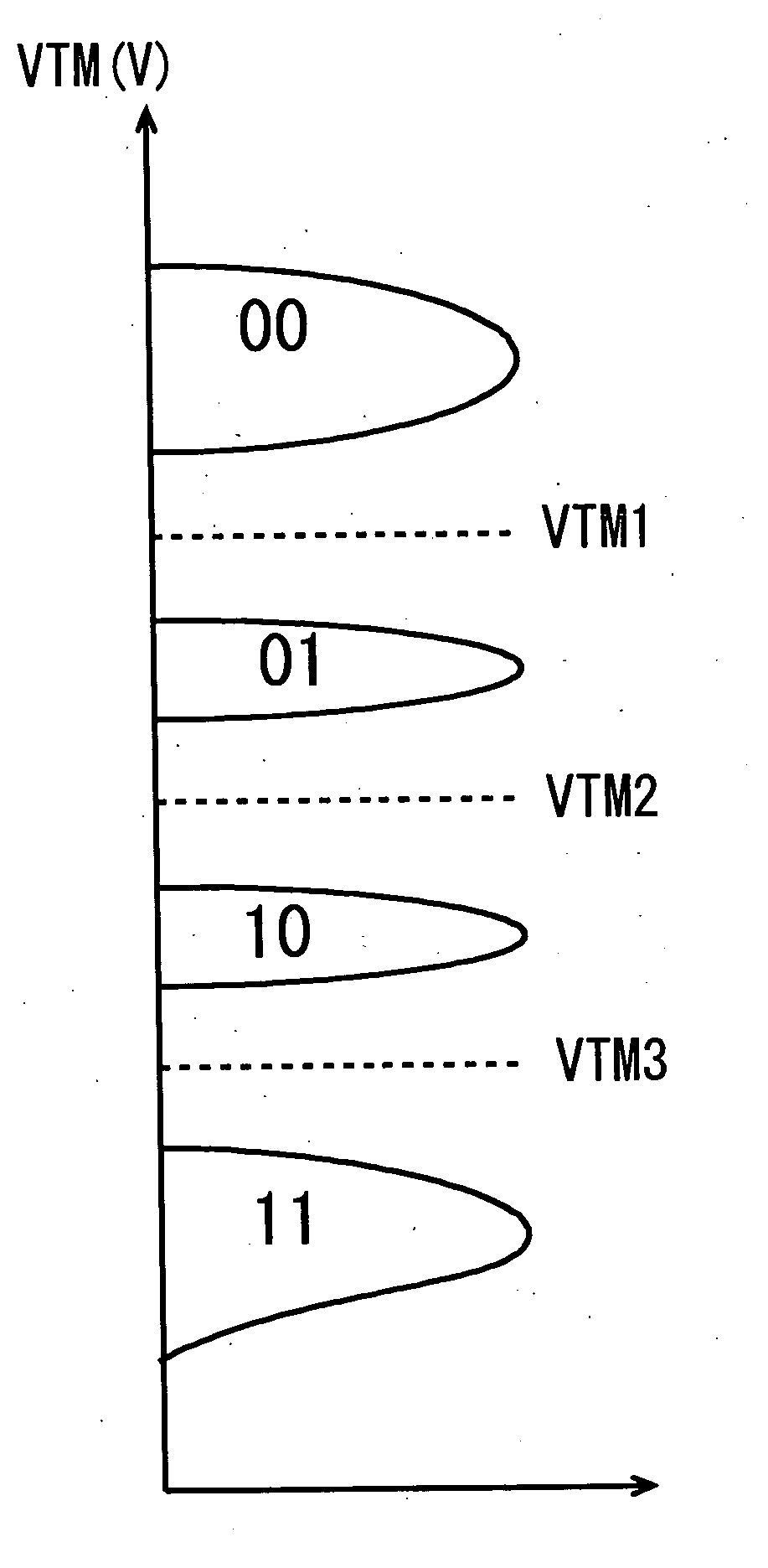
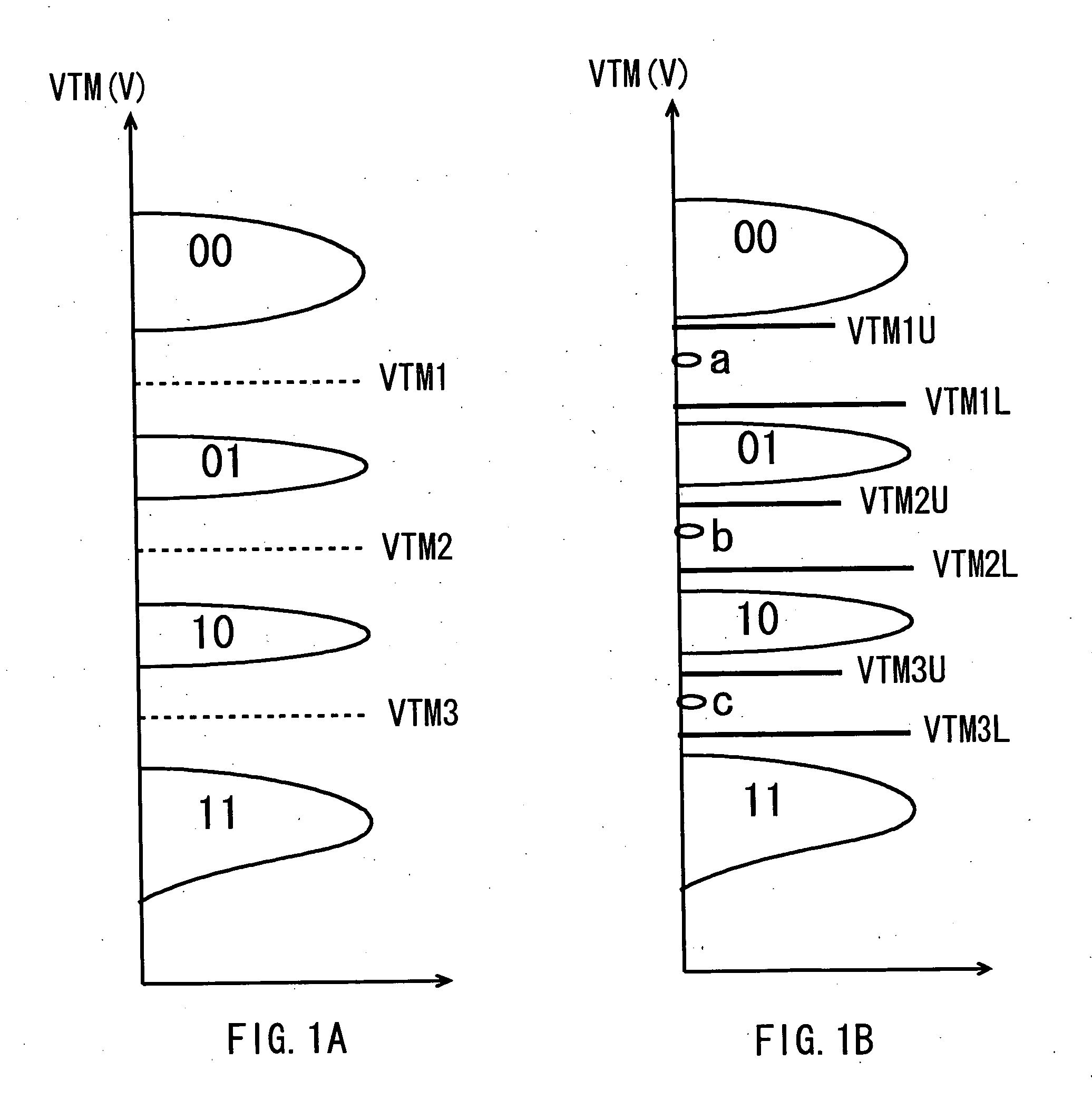
[0032] With the flash memory of this embodiment, cells with defective charge retention are detected, and the defective cells or the data stored in the defective cells are rescued by storing data stored in the defective cells in redundant cells (reserved cells). First, the method of the present embodiment for determining retention defective cells will be described referring to FIGS. 1A-1B. Note, hereinafter, an example where four pieces of data are storted in each multi-value cell will be described. FIG. 1A shows a reference value (VTM(k)) for determining each logical value and a threshold value distribution (transistor threshold voltage) for a 4 value cell in a flash memory. FIG. 1B similarly shows a reference value (VTM(k)) for determining each logical value and a threshold value distribution for a 4 value cell in the flash memory of the present embodiment. The Y axis in each of the figures shows the cell threshold value, and the X axis shows the number of cells. The threshold valu...

embodiment 2

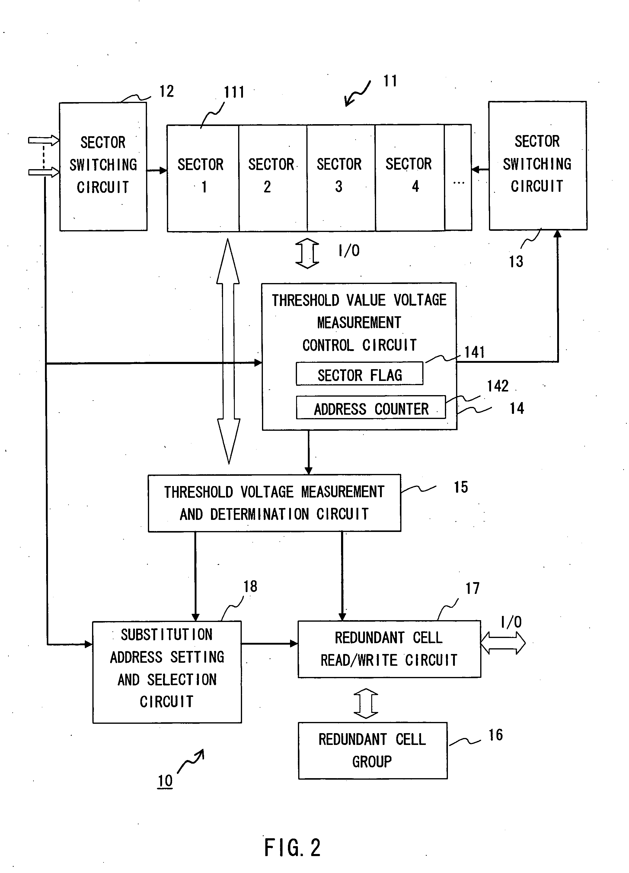
[0047]FIG. 3 shows another embodiment of the memory device of the present invention. In the above example, defective cell check and substitution was performed for each data writing cycle to the memory cell array 11. The memory cell is accessed during the defective cell check. Therefore, from the viewpoint of reducing the load on the memory cell and reducing power consumption, checking for defective cells at a specified interval is preferable. Memory device 20 of the present embodiment checks defective cells each time a designated number of reads or writes processes are performed. Therefore, additional load on the memory cell and additional power consumption can be limited while still performing the necessary defective cell rescues.

[0048] Memory device 20 comprises a command counter 21. The command counter 21 counts the number of read commands and write commands issued (number of command acquisitions) to the memory cell array 11. The counted data is input to the threshold voltage me...

embodiment 3

[0054] In the above embodiment, the defective cell check process is performed depending on the number of acquired commands. However, depending on the memory device, access to the memory cell array may be extremely limited. In these cases, a situation can be imagined where the memory cell array check is not carried out within the necessary time period. The memory device of this embodiment inspects the main cell array when the memory device is powered on or when the memory device is selected and activated by a control signal after it is turned on. Therefore, the memory cell threshold value can be prevented from changing to a different logical value range.

[0055] The memory device 25 comprises a power voltage detection circuit 26. The power voltage detection circuit 26 detects whether or not the power voltage of the memory device 25 is above a reference value, and if the power is detected to be ON, the threshold voltage measurement control circuit 14 will receive a control signal. If t...


PUM


Abstract

The memory device according to an embodiment of the invention prepares a reference field (reference value range) corresponding to each logical value and if the threshold value of the cell is within that field, the cell is determined to be defective and the data of the defective cell is stored in a redundant cell. Therefore, if the threshold value drops because the cell charge leaks over time, the data which is stored can be rescued. As a background operation of a normal operating, memory device performs the memory cell check and memory cell substitution in accordance with the internal addresses generated independently than external addresses. Therefore, a defective cell can be rescued without causing delay in the normal operations of memory device.

Description

BACKGROUND OF THE INVENTION [0001] 1. Field of the Invention [0002] The present invention relates to a nonvolatile memory, and more particularly to a nonvolatile memory which stores data from a memory cell in which an error is detected, in a redundant cell (reserved cell). [0003] 2. Description of the Related Art [0004] Nonvolatile semiconductor memory such as EEPROM and flash memory can be electrically erased or written over, and because the data is not deleted even though the power is turned off, these devices are used in many applications such as portable phones, digital cameras, and personal computer BIOS memory or the like. With this type of nonvolatile semiconductor memory device, a charge is accumulated in a memory cell floating gate and data is stored by changing the cell threshold value. In order to read the data, a current is supplied to the cell, and the data stored in the memory cell can be read by detecting the current value (or threshold value thereof). [0005] When mem...

Claims


Application Information

Patent Timeline
Patent Type & Authority Applications(United States)
IPC IPC(8): G11C11/34G11C16/06G11C16/02G11C16/08G11C16/34G11C29/00G11C29/04
CPCG11C11/5628G11C16/04G11C16/3454G11C16/3459G11C29/00G11C29/50G11C29/50004G11C29/82G11C2029/0409G11C2211/5621
Inventor FURUTA, HIROSHIHASHIMOTO, KIYOKAZU
Owner RENESAS ELECTRONICS CORP
Why Eureka
Try Eureka