Method of manufacturing a semiconductor device and semiconductor device

Inactive Publication Date: 2005-12-08
KK TOSHIBA
View PDF25 Cites 27 Cited by
  • Summary
  • Abstract
  • Description
  • Claims
  • Application Information

AI Technical Summary

Benefits of technology

[0010] According to another aspect of the present invention, provided is a method of manufacturing a semiconductor device, including: immersing a substrate having a recessed portion in a surface thereof, in a plating solution in a plating solution bath, and supplying the plating solution into the plating solution bath at a supply rate of 15 L/min or higher while rotating the substrate at a rotation speed of 50 rpm or lower, thereby forming a metal film on the substrate by a plating method so as to bury the metal film in at least part of the recessed portion; and removing the metal film except a port

Problems solved by technology

Unlike Al, Cu is difficult to process by RIE (reactive ion etching).
This problem is correlated with film deposition rate, and more impurities are mixed in wide wiring trenches in which the bottom-up deposition is difficult to occur than in narrow wiring trenches in which the bottom-up deposition prominently occurs.

Method used


Image

  • Method of manufacturing a semiconductor device and semiconductor device
  • Method of manufacturing a semiconductor device and semiconductor device
  • Method of manufacturing a semiconductor device and semiconductor device

Examples


first embodiment

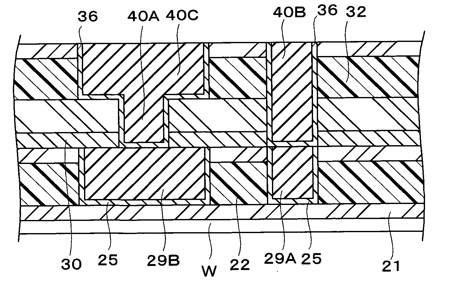
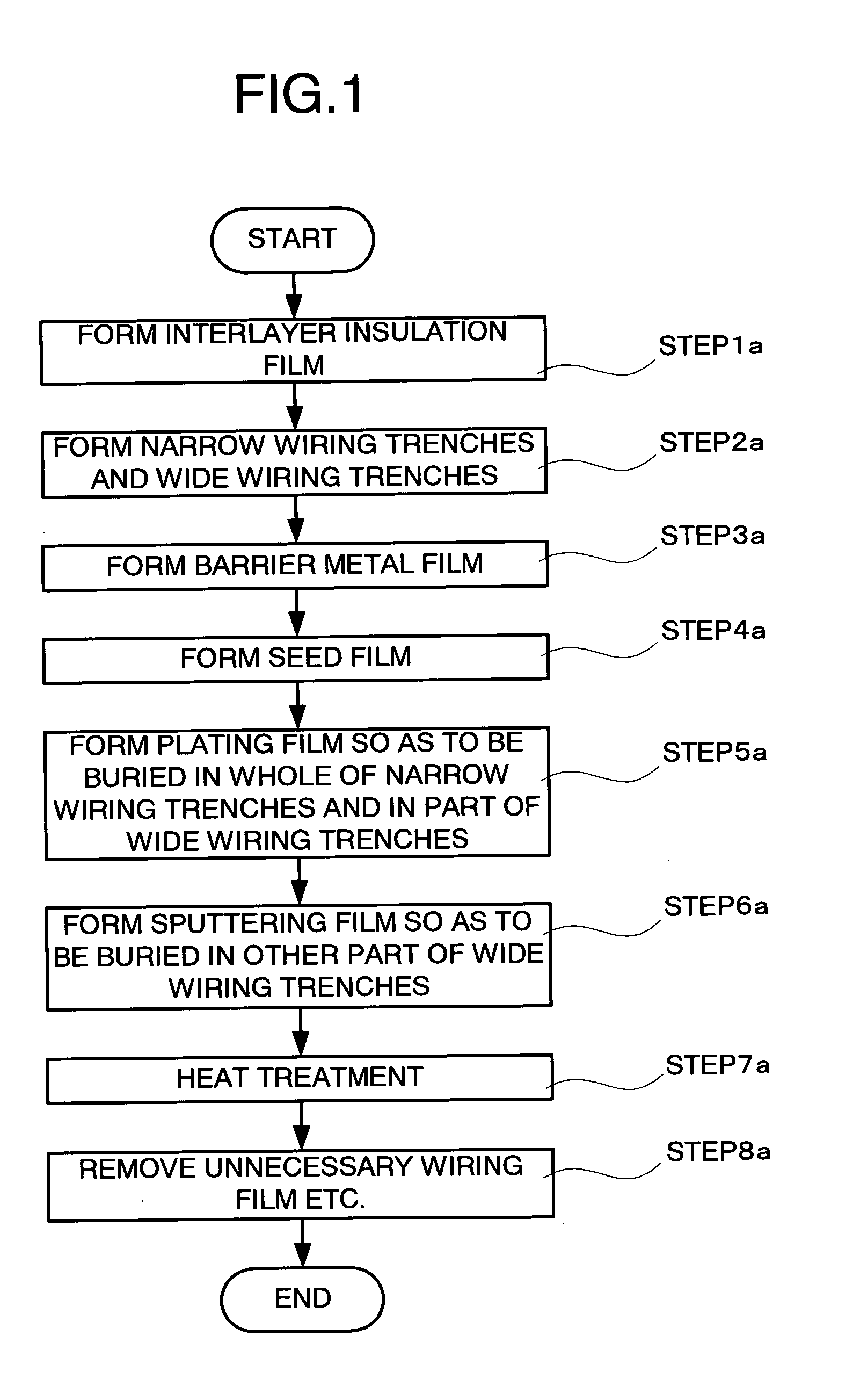
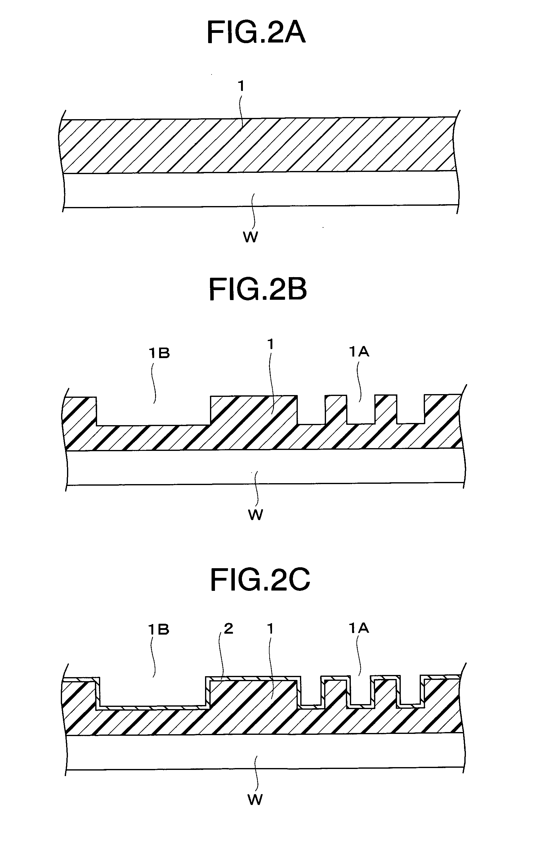
[0023] Hereinafter, a first embodiment will be described. FIG. 1 is a flowchart showing a flow of manufacturing processes of a semiconductor device according to this embodiment, and FIG. 2A to FIG. 2H are schematic views showing the manufacturing processes of the semiconductor device according to this embodiment. formed on a semiconductor wafer W (hereinafter, simply referred to as a “wafer”) by, for example, chemical vapor deposition (CVD) or coating (Step 1a). Examples of a material composing the interlayer insulation film 1 are a low dielectric constant insulation film such as an organic Si oxide film, an organic resin film and a porous Si oxide film, a SiO2 film and so on.

[0024] After the interlayer insulation film 1 is formed, narrow wiring trenches 1A each with a width of 0.3 μm or less and wide wiring trenches 1B each with a width of more than 0.3 μm are formed in the interlayer insulation film 1 as shown in FIG. 2B, by a photolithography technique and reactive ion etching (...

experimental example 1

[0040] Hereinafter, an experiment example 1 will be described. In this experimental example, the impurity concentration in Cu films was measured and defect density in Cu wirings was measured.

[0041] In this experimental example, wafers formed by the following processes were used. After an oxide film was formed to a thickness of 20 nm on each Si substrate having an active portion, a SiOC-based low dielectric constant insulation film (interlayer insulation film) was formed to a thickness of 300 nm by CVD. Thereafter, wiring trenches (wide wiring trenches) each with a width of 4 μm and a depth of 250 nm were formed by lithography processes and RIE processes. Then, after resist removal by a wet etching process, a Ta film (barrier metal film) and a Cu film (seed film) were formed to 30 nm and 80 nm respectively by long throw sputtering. Next, by two kinds of film deposition methods, Cu films were formed. In a condition 1, a Cu film (plating film) was formed to a thickness of 210 nm by el...

second embodiment

[0045] Hereinafter, a second embodiment will be described. This embodiment will describe an example where a plating film is formed by supplying a plating solution at a supply rate of 15 L / min or higher while rotating a wafer at a rotation speed of 50 rpm or lower. Some of the same contents as those in the first embodiment will be omitted.

[0046]FIG. 3 is a flowchart showing a flow of manufacturing processes of a semiconductor device according to this embodiment, FIG. 4 is a schematic view showing the manufacturing processes of the semiconductor device according to this embodiment, FIG. 5 is a schematic view showing a forming process of a plating film according to this embodiment, FIG. 6 shows the correlation of the concentrations of Cu ions and additives relative to the distance from a surface of a wafer in plating by supplying a plating solution at a supply rate of 15 L / min or higher while rotating the wafer at a rotation speed of 50 rpm or lower, FIG. 7 shows the correlation of th...


PUM


Abstract

According to one aspect of the present invention, provided is a method of manufacturing a semiconductor device, including: forming a first metal film on a substrate having a recessed portion in a surface thereof, by a plating method so as to bury the first metal film in at least part of the recessed portion; forming a second metal film on the first metal film by a film deposition method different from the plating method, the second metal film including, as a main component, a metal that is a main component of the first metal film and containing an impurity whose concentration is lower than concentration of an impurity contained in the first metal film; heat-treating the first and second metal films; and removing the first and second metal films except portions buried in the recessed portion.

Description

CROSS-REFERENCE TO RELATED APPLICATION [0001] This application is based upon and claims the benefit of priority from the prior Japanese Patent Application No.2004-167763, filed on Jul. 4, 2004 and the prior Japanese Patent Application No. 2005-149505 filed on May 23, 2005; the entire contents of which are incorporated herein by reference.BACKGROUND OF THE INVENTION [0002] 1. Field of the Invention [0003] The present invention relates to a method of manufacturing a semiconductor device and a semiconductor device. [0004] 2. Description of the Related Art [0005] As a material of wiring of a semiconductor device, Cu has recently come into use instead of Al in order to lower wiring resistance and improve resistance against migration such as electro migration (EM) and stress migration (SM) that may cause faulty wiring. [0006] Unlike Al, Cu is difficult to process by RIE (reactive ion etching). Therefore, for forming wiring by Cu, a damascene method is used in which trenches or holes are f...

Claims


Application Information

Patent Timeline
IPC IPC(8): H01L21/285H01L21/288H01L21/768H01L31/00
CPCH01L21/2855H01L21/2885H01L21/76801H01L21/76802H01L21/76807H01L21/76835H01L21/76877H01L2924/0002H01L2924/00
Inventor MORITA, TOSHIYUKITOYODA, HIROSHIMATSUI, YOSHITAKAIKEGAYA, FUMITOSHISAKATA, ATSUKOKATATA, TOMIOOMOTO, SEIICHI
Owner KK TOSHIBA
Why Eureka
Try Eureka