Lens structures suitable for use in image sensors and method for making the same

a technology of image sensor and lens structure, which is applied in the direction of semiconductor devices, radio frequency controlled devices, electrical devices, etc., can solve the problems of reducing the optical signal and therefore the sensitivity of the photosensor, and the difficulty of aligning the lens and the photosensor

Inactive Publication Date: 2005-12-15
TAIWAN SEMICON MFG CO LTD
View PDF11 Cites 78 Cited by
  • Summary
  • Abstract
  • Description
  • Claims
  • Application Information

AI Technical Summary

Problems solved by technology

The thick inter-metal dielectric makes it difficult to align the lens and photosensor and insure that the light which passes through the lens, reaches the photosensor.
Furthermore, the interconnect metal disposed within the inter-metal dielectric may reflect incident light further reducing the optical signal and therefore the sensitivity of the photosensor.

Method used


Image

  • Lens structures suitable for use in image sensors and method for making the same
  • Lens structures suitable for use in image sensors and method for making the same
  • Lens structures suitable for use in image sensors and method for making the same

Examples


Embodiment Construction

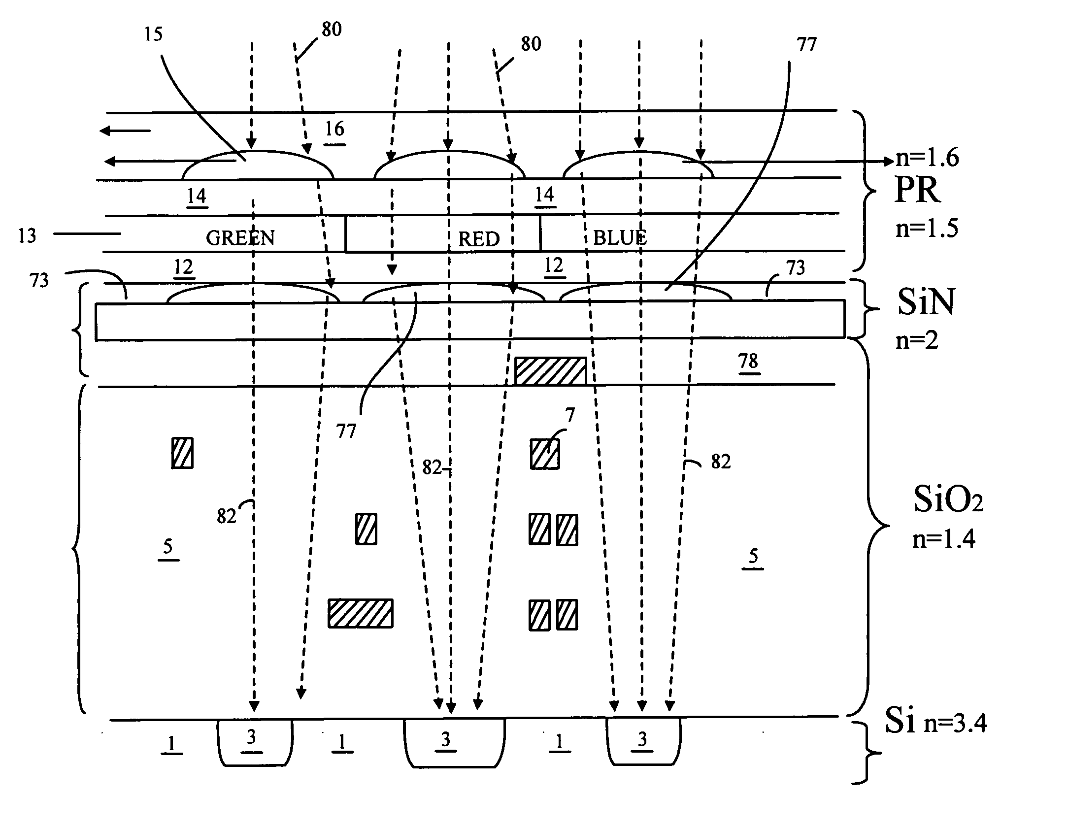
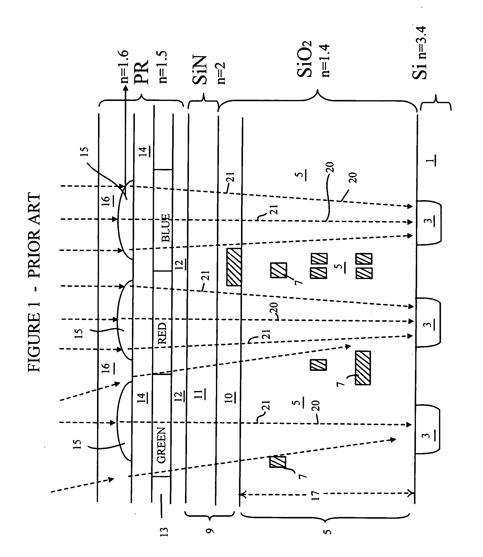
[0021]FIG. 1 shows an exemplary solid state imaging device and includes sensors 3 formed in substrate 1 according to the PRIOR ART. Sensors 3 are photosensitive devices and may be photodiodes or other photosensors. The imaging device also includes inter-metal dielectric, IMD 5 that may include several levels of metal interconnect leads 7 which are desirably disposed between the sensors 3 so as not to deflect or impede light rays 21 from reaching sensors 3. Passivation level 9 may include a silicon nitride film 11 and further dielectric layer 10 which may be formed by the chemical vapor deposition of a high density plasma. The image sensor also includes plain layer 12, color filter 13, microspacer 14 and microlenses 15 aligned over sensors 3. Overcoat 16 covers microlenses 15 and may be formed of suitable materials such as acrylate, methacrylate, epoxy-acrylate, or polyimide and include a thickness of 0.3-3.0 μm. Plain layer 12 may have a refractive index of 1.4-1.7, may be composed ...


PUM


Abstract

An image sensor includes a double-microlens structure with an outer microlens aligned over an inner microlens, both microlenses aligned over a corresponding photosensor. The inner or outer microlens may be formed by a silylation process in which a reactive portion of a photoresist material reacts with a silicon-containing agent. The inner or outer microlens may be formed by step etching of a dielectric material, the step etching process including a series of alternating etch steps including an anisotropic etching step and an etching step that causes patterned photoresist to laterally recede. Subsequent isotropic etching processes may be used to smooth the etched step structure and form a smooth lens. A thermally stable and photosensitive polymeric/organic material may also be used to form permanent inner or outer lenses. The photosensitive material is coated then patterned using photolithography, reflowed, then cured to form a permanent lens structure.

Description

RELATED APPLICATION [0001] This application is related to, and claims priority from U.S. provisional patent application Ser. No. 60 / 578,529, filed Jun. 10, 2004.FIELD OF THE INVENTION [0002] The present invention relates, most generally, to a solid state imaging device, and more particularly to lenses used in such imaging devices and methods for making the same. BACKGROUND [0003] Solid state imaging devices typically include a photosensor such as a photodiode formed in or on a substrate, a color filter formed over the photosensitive device and a microlens array formed over the color filter. The photosensor may be a photodiode, a CMOS (complimentary metal oxide semiconductor) sensor or a charge-coupled device (CCD), for example. N+ type photosensors (NPS's) are commonly used. Between the photosensor and the color filter there is generally a relatively thick inter-metal dielectric (IMD) that accommodates multiple levels of metallization used as an interconnection medium in the periphe...

Claims


Application Information

Patent Timeline
Patent Type & Authority Applications(United States)
IPC IPC(8): H01L21/00H01L27/146H01L29/04H01L29/06H01L29/10H01L29/22H01L29/227H01L31/036H01L31/0376H01L31/20H01L33/00H01L47/02
CPCH01L27/14621H01L27/14625H01L27/14627H01L27/14632H01L27/14685H01L27/14687
Inventor KUO, CHING-SENSHIU, FENG-JIASHIAU, GWO-YUHCHEN, JIEH-JANGFU, SHIH-CHITSENG, CHIEN HSIENTSAI, CHIA-SHIUNGLIU, YUAN-HUNGTU, YEUR-LUENWU, CHIH-TALO, CHI-HSIN
Owner TAIWAN SEMICON MFG CO LTD
Why Eureka
Try Eureka