
ESD protection for integrated circuits

a technology of integrated circuits and protection devices, applied in the direction of semiconductor devices, semiconductor/solid-state device details, electrical apparatus, etc., can solve problems such as defective or useless rendering, and achieve the effects of improving the inherent bipolar transistor gain of the structure, increasing the gain, and increasing the gain

Inactive Publication Date: 2005-12-15
MICREL
View PDF5 Cites 35 Cited by
  • Summary
  • Abstract
  • Description
  • Claims
  • Application Information

AI Technical Summary

Benefits of technology

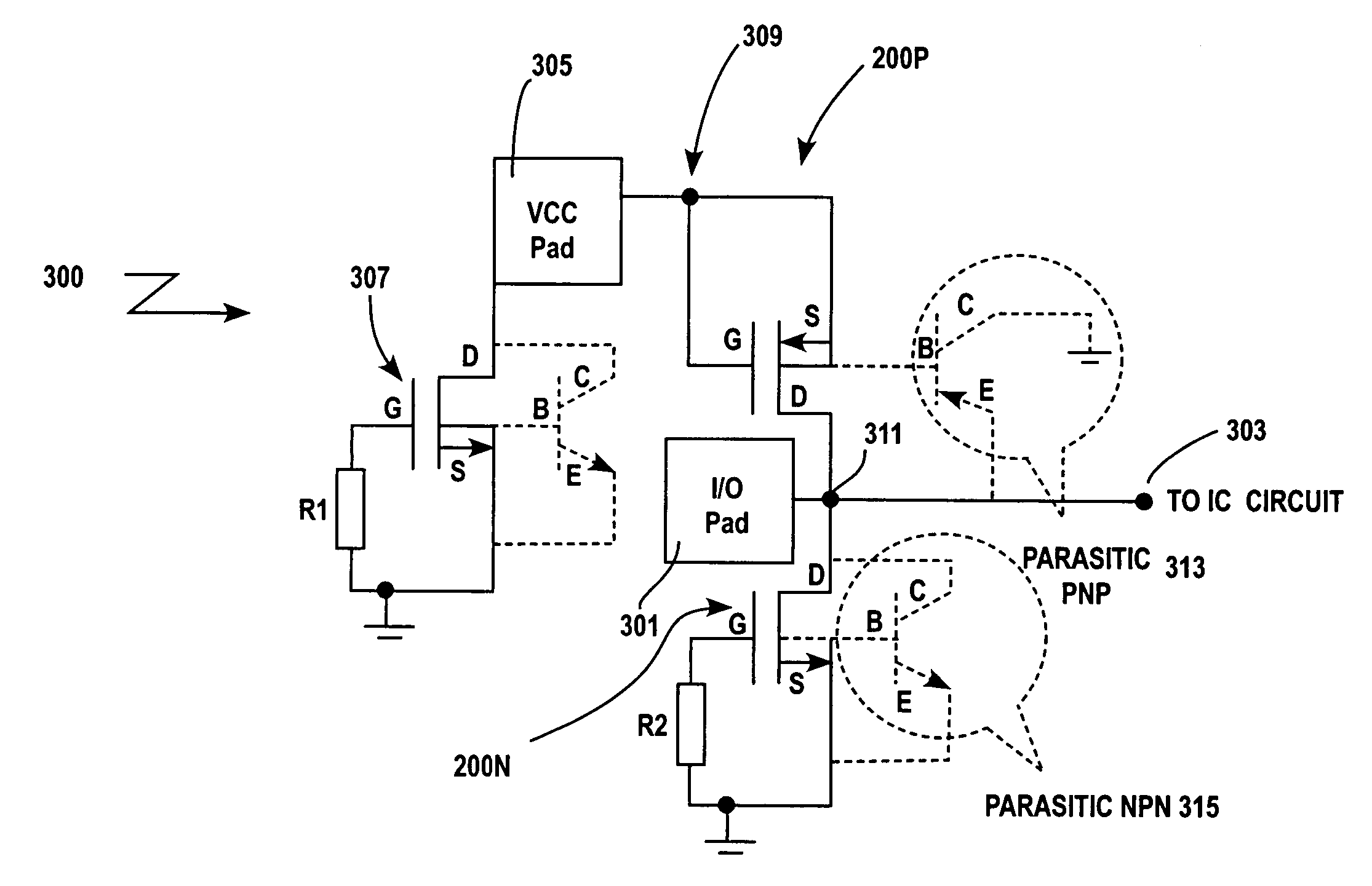
[0012] In one aspect, an exemplary embodiment of the present invention provides semiconductor MOSFET structure having improved ESD tolerance, the structure including: a semiconductor substrate having an active device surface; in said surface, a MOSFET source region and a MOSFET drain region separated by a channel region; a P-type dopant region subjacent said drain region and having a dopant concentration and predetermined dimensions such inherent parasitic transistor gain of said MOSFET structure is increased.
[0022] In another aspect, an exemplary embodiment of the present invention provides an extended drain N-channel MOSFET structure including: a P-type substrate; in said substrate at least one MOSFET structure having extended and enhanced drain region devices for providing reduced on-resistance at a surface region of said substrate, said MOSFET structure including an N+ doped drain region in an N-type well region; and a P-deep region subjacent the N-well containing the drain region, said P-deep region having geometry and a dopant concentration such that said P-deep region increases gain of a parasitic lateral NPN transistor and lowers triggering voltage of said MOSFET.

Problems solved by technology

Such ESD spikes can damage or destroy the IC components, rendering it defective or useless.

Method used


Image

  • ESD protection for integrated circuits
  • ESD protection for integrated circuits
  • ESD protection for integrated circuits

Examples


Embodiment Construction

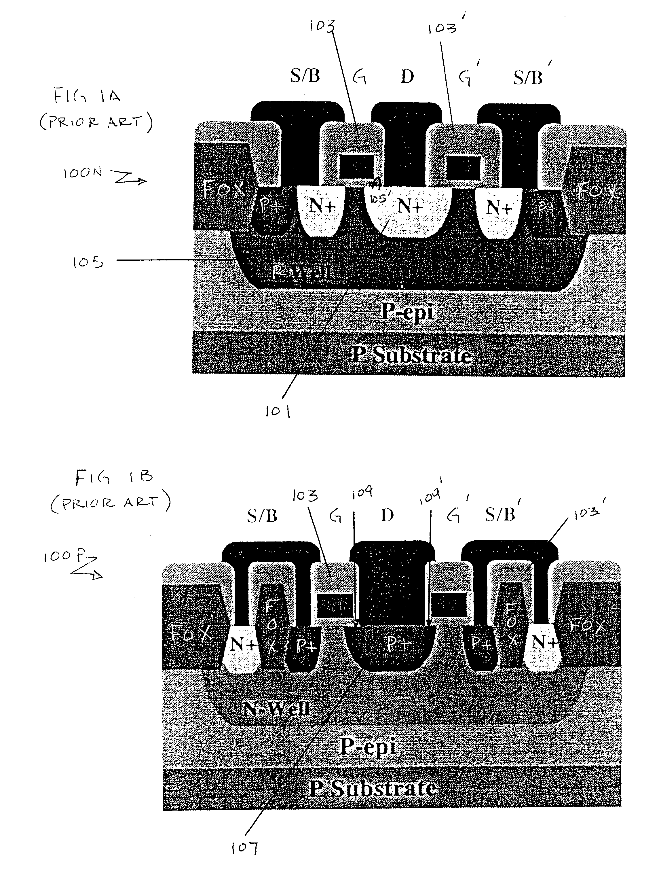
[0038] In general, the present invention uses at least one P-type, implantation region, or layer, referred to hereinafter as “P-deep,” in both NMOS and PMOS devices to enhance ESD protection performance. The present invention is particularly suited to enhancing ESD protection performance for I / O cells and power supply clamps used in CMOS and BiCMOS IC technologies.

[0039] A cross-sectional, elevation view schematic of a pair of adjacent N-MOSFET 200N structures in accordance with an exemplary embodiment of the present invention is shown in FIG. 2A. It should be recognized that this drawing represents a small region of input / output structures of a complete IC, viz., part of an array of I / O cells, or the like as would be known in the art. It should be recognized that many publications describe the details of common techniques used in the fabrication process of integrated circuit components. See, e.g., Wolf, S., Silicon Processing for the VLSI Era, copyright 1990, Lattice Press; Sze, S...


PUM


Abstract

Electrostatic discharge protection for integrated circuits, particularly for enhancing electrostatic discharge protection performance for Input-output cells and power supply clamps used in CMOS and BiCMOS IC technologies is described. A P-type, implantation region, or layer, referred to as “P-deep,” in both N-MOSFET and P-MOSFET devices is provided to enhance electrostatic discharge protection performance. Parasitic transistor gain is enhanced by providing the P-deep region subposing the drain contact. Exemplary embodiments for N-type and P-type MOSFETs, MOSFETs with surface diodes, MOSFETS with SCRs, and push-pull Input-output CMOS circuits are described.

Description

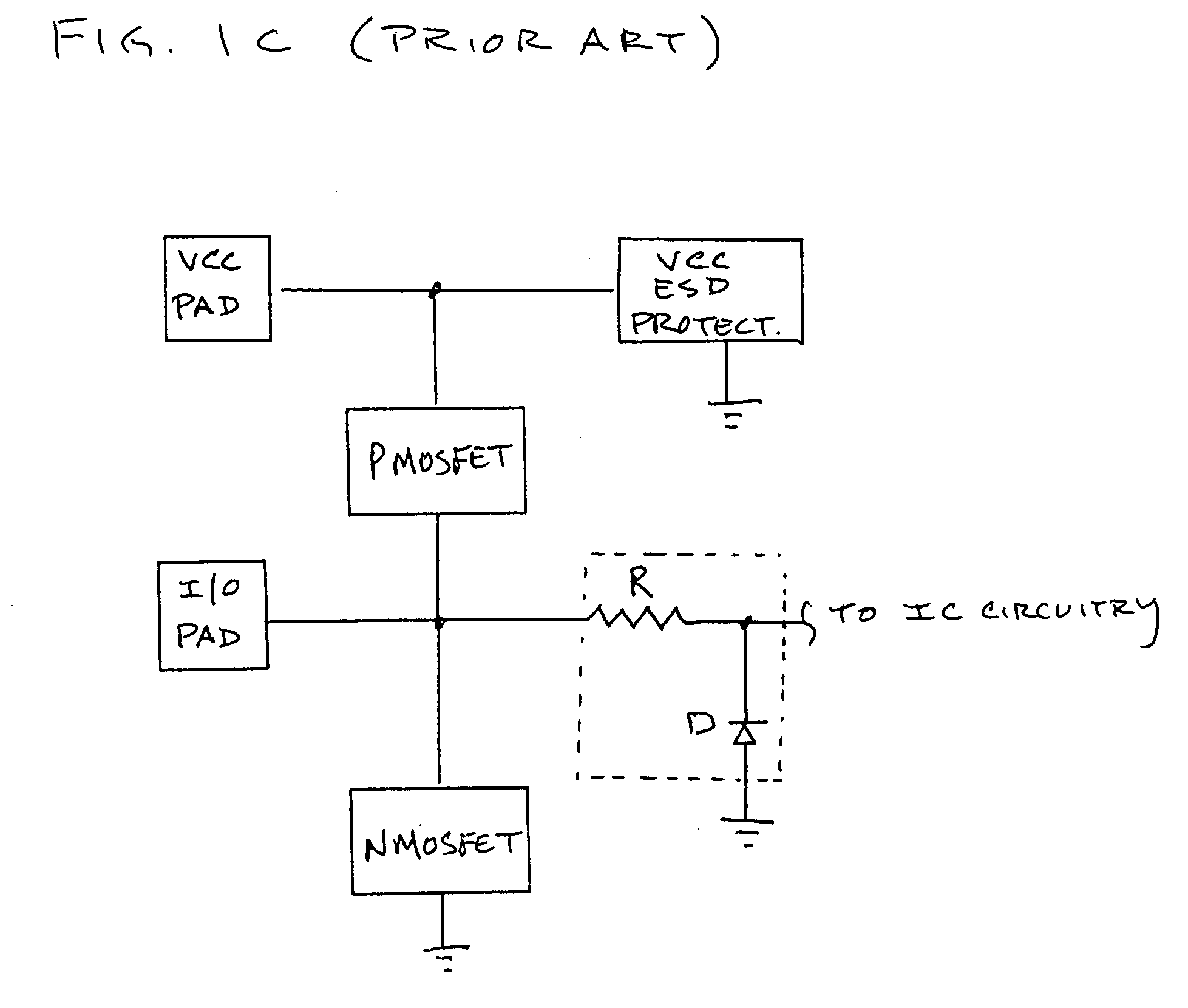
CROSS-REFERENCE TO RELATED APPLICATIONS [0001] Not applicable. STATEMENT REGARDING FEDERALLY SPONSORED RESEARCH OR DEVELOPMENT [0002] Not applicable. REFERENCE TO AN APPENDIX [0003] Not applicable. BACKGROUND TECHNICAL FIELD [0004] This disclosure relates generally to integrated circuits and more particularly to electrostatic discharge protection for integrated circuits. DESCRIPTION OF RELATED ART [0005] Electrostatic discharge (“ESD”) is a well known concern with respect to the design and implementation of integrated circuits (“IC” or “chip”). ESD events occur when very large electrical spikes, potentially reaching thousands of volts, occur on an input-output (“I / O”) terminal, “pad,” of the chip which is designed for an operating voltage of just a few volts. Such ESD spikes can damage or destroy the IC components, rendering it defective or useless. Therefore, ICs are frequently designed to provide some sort of protection against ESD events. [0006] The ESD problem is particularly eg...

Claims


Application Information

Patent Timeline
Patent Type & Authority Applications(United States)
IPC IPC(8): H01L23/62
CPCH01L27/0266H01L29/0649H01L29/0653H01L29/0847H01L29/0852H01L29/78H01L2924/0002H01L29/1083H01L2924/00
Inventor MALLIKARJUNASWAMY, SHEKAR
Owner MICREL
Learn More