Method of forming a lead-free bump and a plating apparatus therefor
Inactive Publication Date: 2005-12-22
SHIMOYAMA MASASHI +4
View PDF3 Cites 22 Cited by
Summary
Abstract
Description
Claims
Application Information
AI Technical Summary
This helps you quickly interpret patents by identifying the three key elements:
Problems solved by technology
Method used
Benefits of technology
[0010] It has also been found that contrary to the expectation that a decrease in the Ag content of a plated alloy film from the Ag content of the Sn—Ag eutectic composition will incur a rise in the
Problems solved by technology
With printing, however, there is a limit in its approach to fine pitches through the use of a metal mask.
However, the formation of bumps by electroplating has the problem tha
Method used
Image
Click on the blue label to locate the original text in one second.
Reading with bidirectional positioning of images and text.
Examples
example 1
(1) Preparation of Sn—Ag Bump:
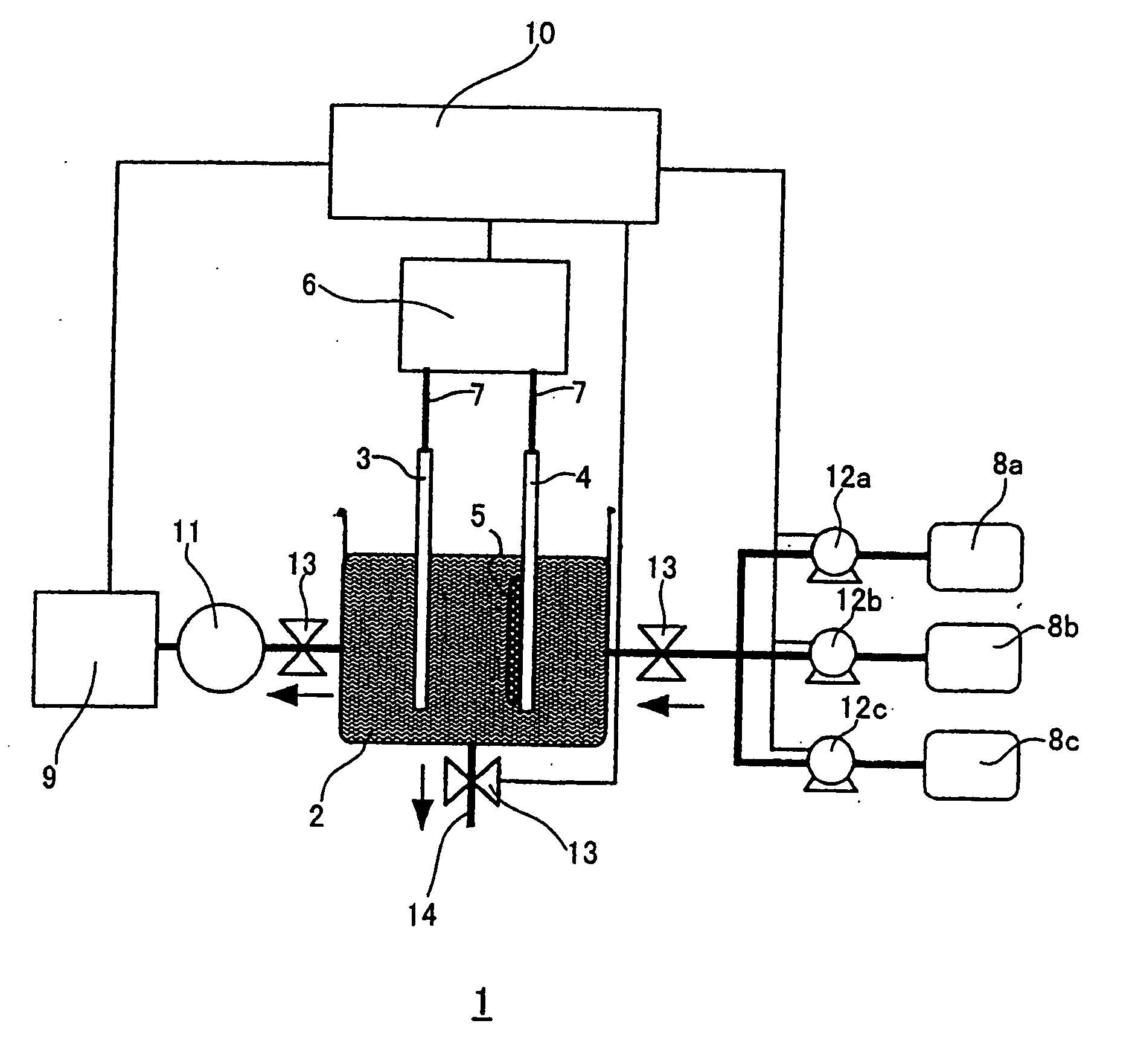
[0067] A resist was applied to a thickness of 120 μm on a wafer in such a manner that a number of holes having an opening size of 100 μm are formed, thereby preparing a sample. The plating area of the sample was 149.63 cm2. Plating of the sample was carried out by the following steps under the following conditions.
[0075] Circulation of plating solution: flow rate 2.5 L / min
[0076] Electrode: copper anode, interpolar distance about 7.5 mm, anode mask ø 250 mm
[0077] Cathode current density (total current): 5 A / dm2 (7.48 A)
[0078] Plating thickness: 2 μm
[0079]...
example 2
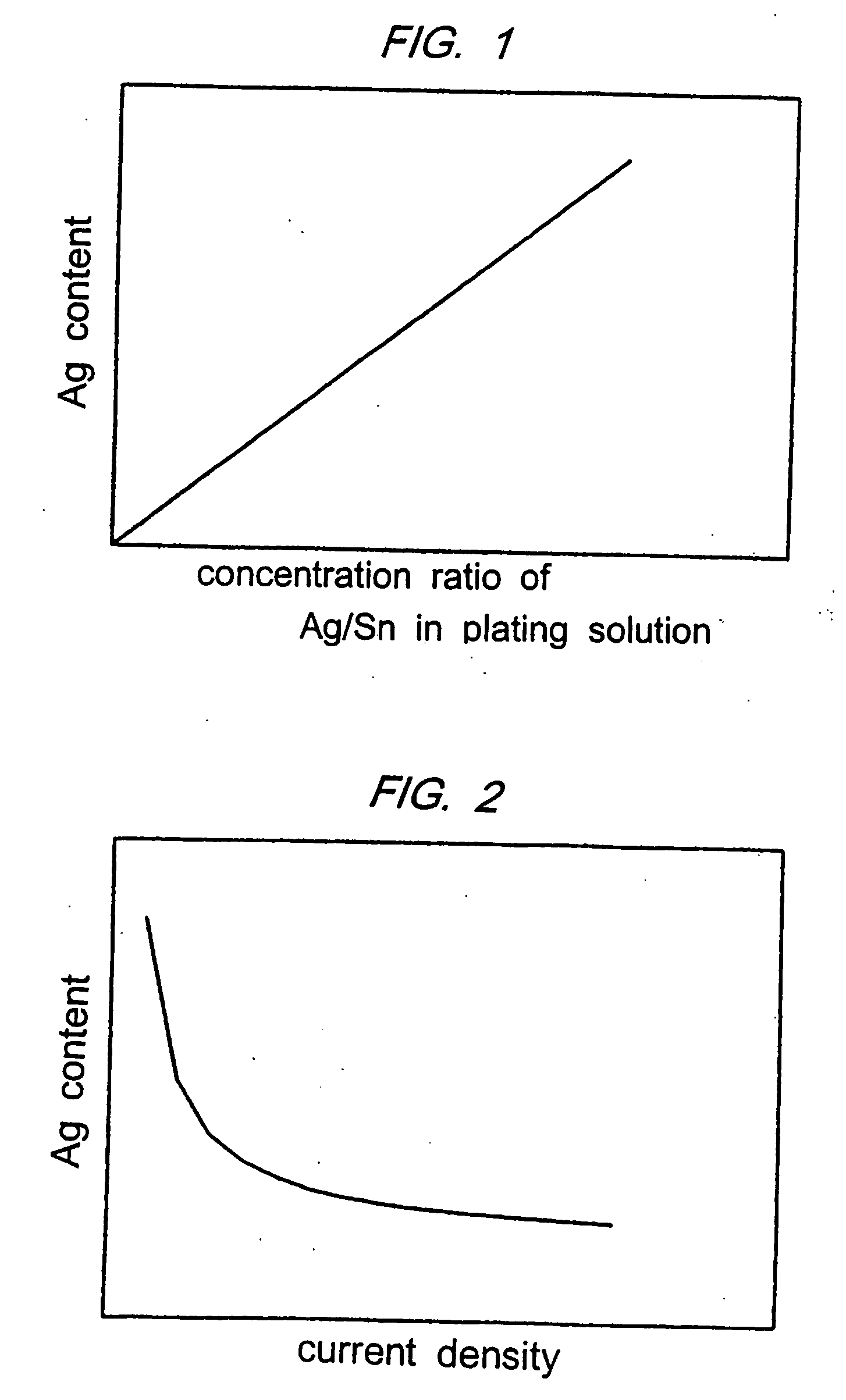
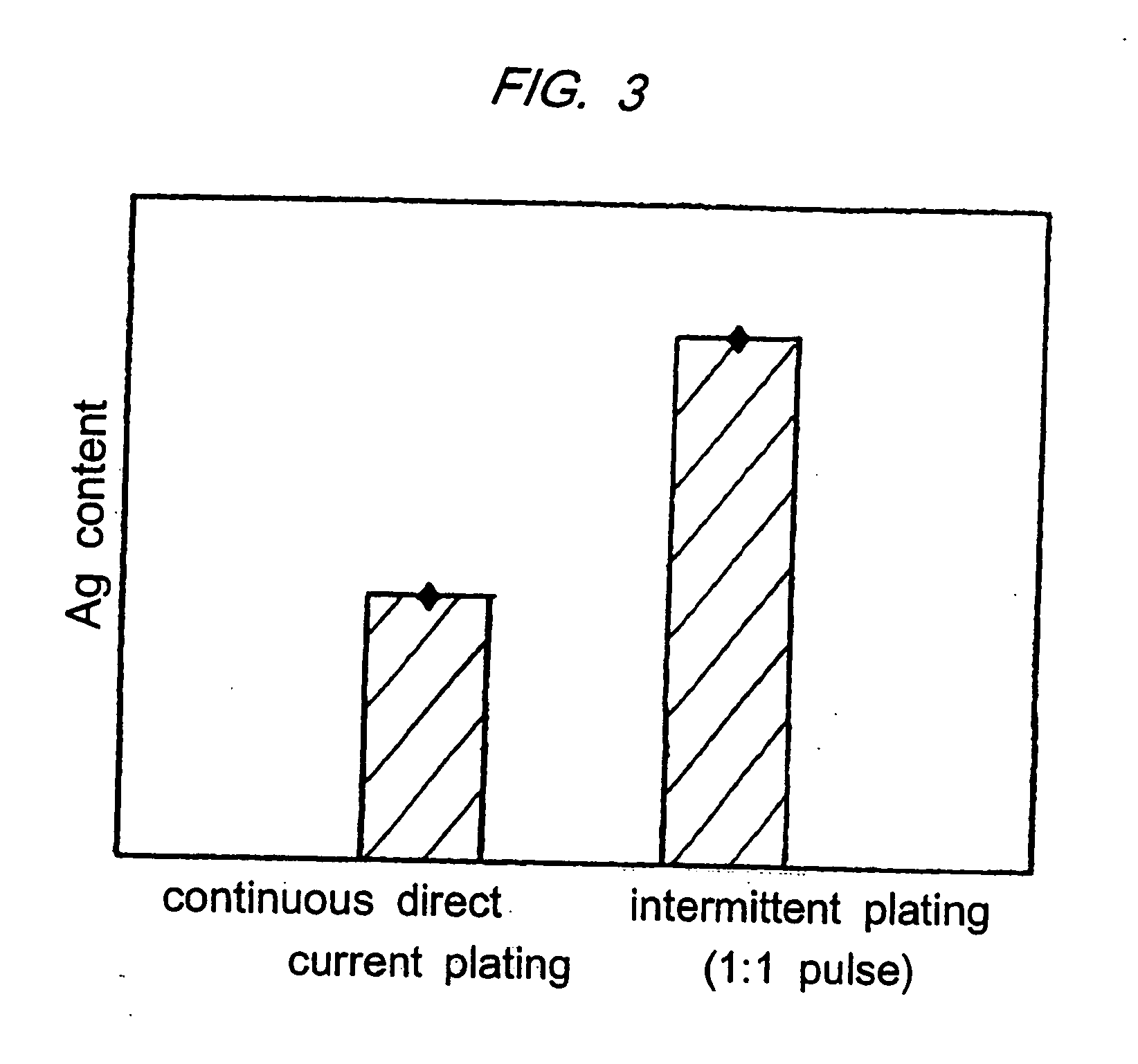
[0102] Alloy plating was carried out with various proportions of Ag to the total metal in an alloy plating solution, various current densities upon plating and various current application methods, and the respective plated alloy films were subjected to reflowing at 238° C. For the bump thus obtained, measurement of the Ag content and observation of the shape of bump and the presence of voids were carried out in the same manner as in Example 1. The results are shown in table 1.
DC denotes direct current plating, and CHOP denotes intermittent plating
[0103] As apparent from the results shown in Table...
PUM
Property
Measurement
Unit
Temperature
aaaaa
aaaaa
Percent by mass
aaaaa
aaaaa
Volume
aaaaa
aaaaa
Abstract
The present invention relates to a lead-free bump with suppressed formation of voids, obtained by reflowing a plated film of Sn—Ag solder alloy having an adjusted Ag content, and a method of forming the lead-free bump. The lead-free bump of the present invention is obtained by forming an Sn—Ag alloy film having a lower Ag content than that of an Sn—Ag eutectic composition by plating and reflowing the plated alloy film.
Description
BACKGROUND OF THE INVENTION [0001] 1. Field of the Invention [0002] The present invention relates to a lead-free bump and a method of forming the same, and more particularly to a lead-free bump with suppressed formation of voids, obtained by reflowing a plated film of Sn—Ag solder alloy having an adjusted Ag content, and a method of forming the lead-free bump, and also to a plating apparatus for forming such a lead-free bump. [0003] 2. Description of the Related Art [0004] In surface mounting technology of semiconductor devices or the like, it is very important to carry out soldering with high reliability. Although an eutectic solder containing lead (Sn:Pb=63:37) has heretofore been used widely in soldering, in the light of environmental contamination and because of the problem of α-rays generation from lead, development of lead-free soldering is under way. [0005] For example, lead-free soldering by means of printing or electroplating is being studied. With printing, however, there ...
Claims
Application Information
Patent Timeline
Application Date:The date an application was filed.
Publication Date:The date a patent or application was officially published.
First Publication Date:The earliest publication date of a patent with the same application number.
Issue Date:Publication date of the patent grant document.
PCT Entry Date:The Entry date of PCT National Phase.
Estimated Expiry Date:The statutory expiry date of a patent right according to the Patent Law, and it is the longest term of protection that the patent right can achieve without the termination of the patent right due to other reasons(Term extension factor has been taken into account ).
Invalid Date:Actual expiry date is based on effective date or publication date of legal transaction data of invalid patent.