Magnetic random access memory array with coupled soft adjacent magnetic layer

Inactive Publication Date: 2005-12-22
HEADWAY TECH INC
View PDF10 Cites 10 Cited by
  • Summary
  • Abstract
  • Description
  • Claims
  • Application Information

AI Technical Summary

Benefits of technology

[0008] Chen et al. (U.S. Pat. No. 5,966,323) teaches a MTJ MRAM cell that can be switched with a low applied field by forming magnetic layers coupled in antiparallel directions so that the cell, as a whole, has no magnetic moment.
[0009] Inomata et al. (U.S. Pat. No. 6,611,405 B1) provide a multi-layer, multi-tunnel junction MRAM device in which a current of spin-polarized electrons flows through the device while bit and word lines also carry current. The arrangement allows an easier reorientation of the magnetic moments with lower currents.
[0010] Engel et al. (U.S. Pat. No. 6,531,723 B1) teach the formation of an MRAM cell in which the free layer is a multi-layered laminate of antiferromagnetically coupled layers. Increasing the number of layers in the laminate increases the magnetic switching volume of the cell so that the energy barrier that must be exceeded in order to inadvertently switch the magnetization direction is increased.
[0011] Another way to address the problem that high currents are needed to change th

Problems solved by technology

Parkin also notes that such small sizes are associated with significant problems, particularly super-paramagnetism, which is the spontaneous, thermal fluctuation of magnetization in samples of ferromagnetic material too small to have sufficient magnetic anisotropy (a measure of the ability of a sample to maintain a given magnetization direction).
Unfortunately, the size of the switching field increases with layer thickness, so the price paid for a thermally stable cell is the necessity of expending a great deal of current to change the magnetic orientation of the cell's free layer.
Yet this form of anisotropy brings with it its own pro

Method used


Image

  • Magnetic random access memory array with coupled soft adjacent magnetic layer
  • Magnetic random access memory array with coupled soft adjacent magnetic layer

Examples


Embodiment Construction

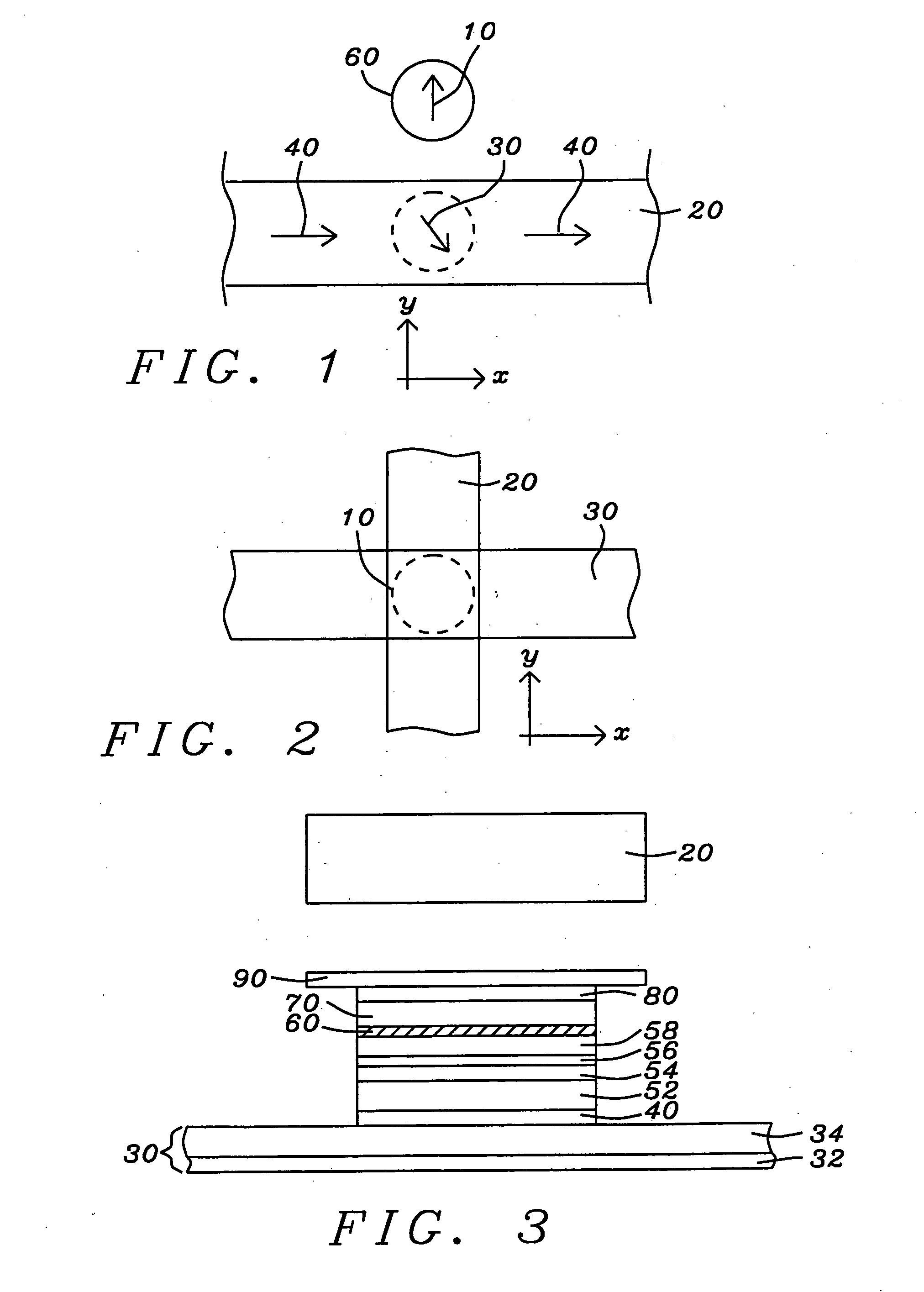
[0021] The preferred embodiment of the present invention teaches a method of forming an MTJ MRAM cell of substantially circular cross-section or an MRAM array of such cells, in which the required switching current in the bit line can be reduced by the addition of a thin adjacent soft magnetic layer beneath the bit line which couples magnetostatically to a proximal free layer.

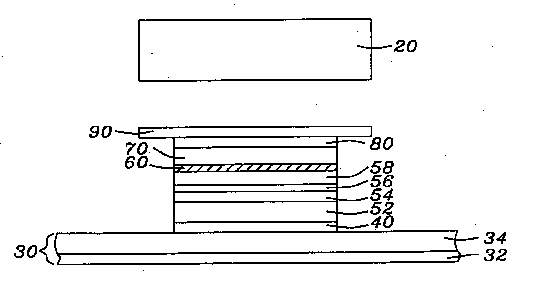
[0022] Referring first to FIG. 2 there is shown in a schematic overhead view in the xy-plane, the general layout of the MRAM cell of the present invention. The MTJ element (10), of substantially circular or low aspect ratio (20), which is above the cell and runs in the y-direction, and a bit line (30), which is below the cell and runs in a direction perpendicular to the write word line (the x-direction). The combination of the MTJ element and the write word and bit lines which access and switch the cell form an MTJ MRAM cell. As will be shown in the next figure, a soft magnetic layer is formed on the bottom sur...


PUM

PropertyMeasurementUnit
Thicknessaaaaaaaaaa
Thicknessaaaaaaaaaa
Antiferromagnetismaaaaaaaaaa

Abstract

An MTJ element is formed between orthogonal word and bit lines. The bit line is a composite line which includes a high conductivity layer and a soft magnetic layer under the high conductivity layer. During operation, the soft magnetic layer concentrates the magnetic field of the current and, due to its proximity to the free layer, it magnetically couples with the free layer in the MTJ. This coupling provides thermal stability to the free layer magnetization and ease of switching and the coupling may be further enhanced by inducing a shape or crystalline anisotropy into the free layer during formation.

Description

BACKGROUND OF THE INVENTION [0001] 1. Field of the Invention [0002] This invention relates to the design and fabrication of magnetic tunnel junctions (MTJ) as memory storage devices, particularly to a design wherein a soft-magnetic adjacent layer is included as part of a composite bit line. [0003] 2. Description of the Related Art [0004] The magnetic tunnel junction (MTJ) basically comprises two electrodes, which are layers of ferromagnetic material, separated by a tunnel barrier layer, which is a thin layer of insulating material. The tunnel barrier layer must be sufficiently thin so that there is a probability for charge carriers (typically electrons) to cross the layer by means of quantum mechanical tunneling. The tunneling probability is spin dependent, however, depending on the availability of tunneling states with different electron spin orientations. Thus, the overall tunneling current will depend on the number of spin-up vs. spin-down electrons, which in turn depends on the ...

Claims


Application Information

Patent Timeline
IPC IPC(8): A61K31/404C07D209/08G11C11/16H01L27/22H01L43/08
CPCH01L43/08G11C11/16G11C11/1655G11C11/1675G11C11/1659G11C11/161G11C11/1657H10N50/10
Inventor GUO, YIMINMIN, TAIWANG, POKANGSHI, XIZENG
Owner HEADWAY TECH INC
Why Eureka
Try Eureka