

Back-end-of-line metallization inspection and metrology microscopy system and method using x-ray fluorescence
a metrology microscopy and back-end-of-line technology, applied in the direction of individual semiconductor device testing, semiconductor/solid-state device testing/measurement, instruments, etc., can solve the problems of circuit failure, void creation, and conductor traces breaking
- Summary
- Abstract
- Description
- Claims
- Application Information
AI Technical Summary
Benefits of technology
Problems solved by technology
Method used
Image

Examples
Embodiment Construction
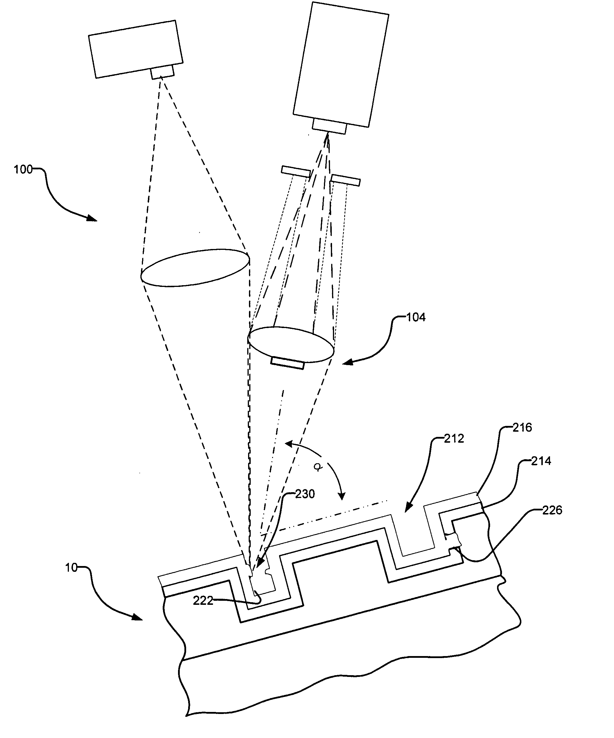
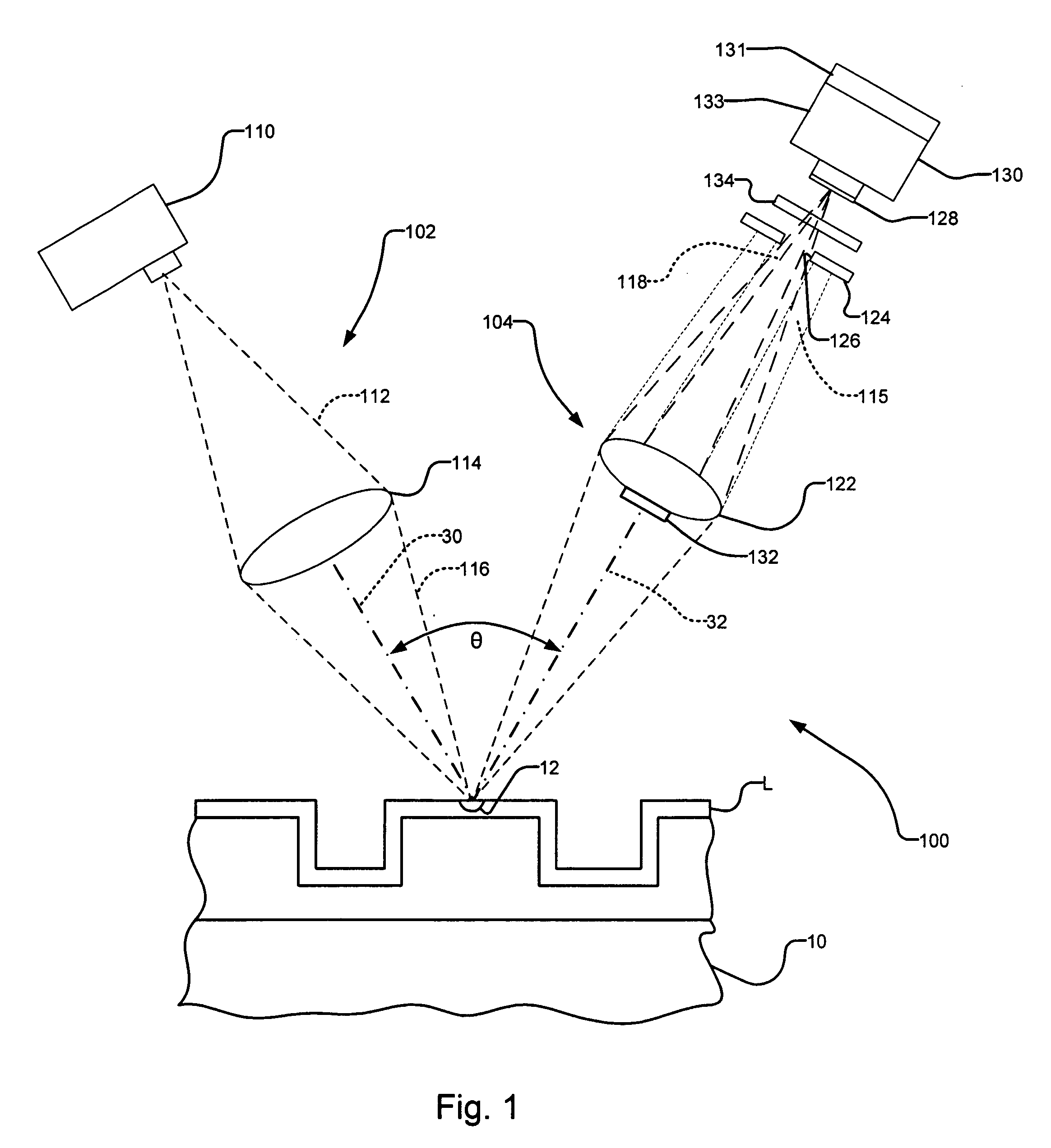
[0022] The preferred embodiment of the invention concerns an x-ray fluorescence metallization analysis system for the inspection and metrology of the barrier and seed layers for metallization processes such as during and after Damascene processes. It also concerns the detection, measurement and other characterization of void formation during or after the deposition, such as by electroplating, of interconnect structures, such as interconnects formed from copper.
[0023]FIG. 1 illustrates an x-ray metallization analysis system 100 that has been constructed according to the principles of the present invention.
[0024] The system 100 comprises an excitation system 102 that has an excitation source 110. This excitation source 110 generates a radiation beam that is used to generate the x-ray fluorescence emissions from the sample or device under analysis 10.
[0025] Typically, the excitation radiation 112 is either x-ray radiation or an electron beam. The electron sources include thermionic ...
PUM
 Abstract
Description
Claims
Application Information