Semiconductor device fabrication method

a technology of semiconductor devices and fabrication methods, applied in semiconductor/solid-state device manufacturing, basic electric elements, electric devices, etc., can solve the problems of lowering process yield and uneven transistor characteristics, and achieve the effect of preventing the occurrence of silicon layer dishing and improving process yield

Active Publication Date: 2005-12-22
SHARP KK
View PDF4 Cites 2 Cited by
  • Summary
  • Abstract
  • Description
  • Claims
  • Application Information

AI Technical Summary

Benefits of technology

[0016] According to the invention, while the portion other than projected parts of a silicon layer being protected with an insulating layer, the projected parts of the silicon layer are chemically and mechanically polished and therefore the portion protected with the insulating layer is not removed at the time of polishing and occurrence of dishing of the silicon layer can be prevented.
[0017] Consequently, according to the invention, the silicon layer can precisely be leveled. As a result, the film thickness of the silicon layer in an embedding region can be made even and transistors and wiring can be formed evenly and thus the process yield can be improved.

Problems solved by technology

However, in this method, the polycrystalline silicon layer in the recessed parts of the substrate surface is exposed constantly to the polycrystalline silicon polishing slurry and a polishing pad.
This excess polishing of the silicon layer makes the thickness of the embedded silicon layer to be wiring or electrodes uneven or eliminates the silicon layer regions to result in unevenness of the transistor characteristics and wiring resistance or electrode elimination or wiring disconnection and thus the process yield is lowered.

Method used


Image

  • Semiconductor device fabrication method
  • Semiconductor device fabrication method
  • Semiconductor device fabrication method

Examples


first embodiment

1. First Embodiment

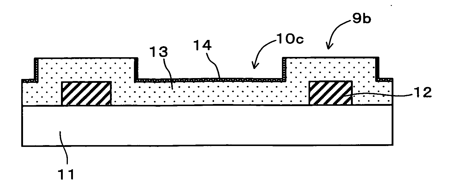
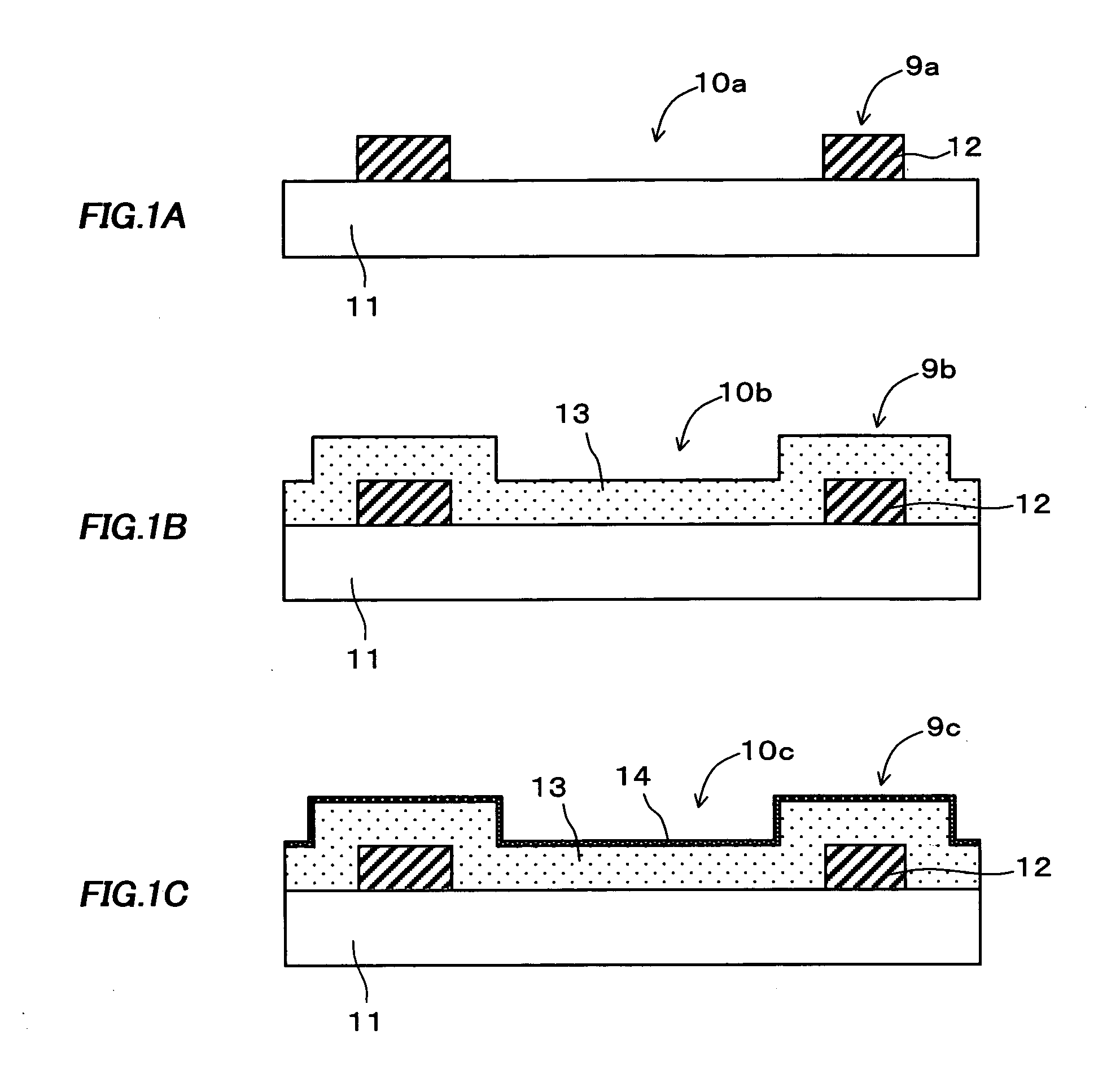
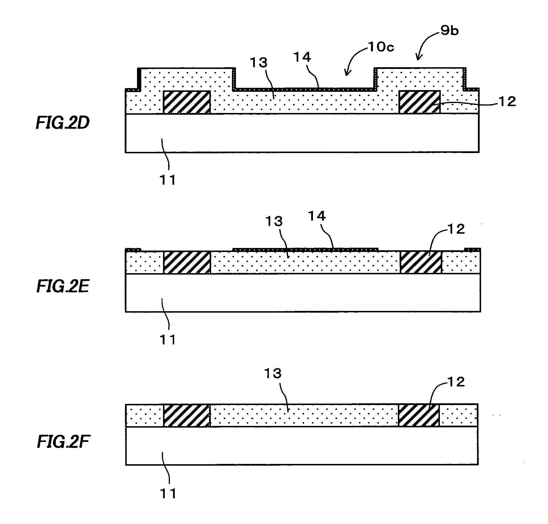
[0024] A semiconductor device fabrication method according to a first embodiment of the invention comprises the steps of: (1) exposing a silicon layer by removing a portion of an insulating layer above a projected part of the silicon layer, the insulating layer covering the silicon layer; and (2) chemically and mechanically polishing the exposed silicon layer with a polishing slurry for the silicon layer while protecting the silicon layer with the remaining of the insulating layer.

1-1. Step of Exposing a Silicon Layer by Removing a Portion of an Insulating Layer Above a Projected Part of the Silicon Layer, the Insulating Layer Covering the Silicon Layer

[0025] A silicon layer may be a polycrystalline silicon layer, an amorphous silicon layer or a single crystal silicon layer. Further, the term “silicon layer” includes a layer of silicon alloy such as silicon germanium.

[0026] A silicon oxide such as silicon dioxide or a silicon nitride can be used for the insula...

second embodiment

2. Second Embodiment

[0034] A semiconductor device fabrication method according to a second embodiment of the invention comprises the steps of: (1) forming a silicon layer having a thickness substantially the same as or thinner than the height of a projected part on a substrate so as to cover the surface of the substrate, the projected part being formed of a first insulating layer; (2) forming a second insulating layer covering the silicon layer; (3) exposing the silicon layer by removing a portion of the second insulating layer above the projected part on the substrate; (4) substantially leveling the silicon layer and exposing the first insulating layer by chemically and mechanically polishing the exposed silicon layer while protecting the silicon layer with the remaining of the second insulating layer and using the remaining of the second insulating layer or the projected part of the first insulating layer as a stopper layer; and (5) removing the remaining of the second insulating ...

third embodiment

3. Third Embodiment

[0049] A semiconductor device fabrication method according to a third embodiment of the invention comprises the steps of: (1) forming a silicon layer having a thickness thicker than the height of a projected part on a substrate so as to cover the surface of the substrate, the projected part being formed of a first insulating layer; (2) forming a second insulating layer covering the silicon layer; (3) exposing the silicon layer by removing a portion of the second insulating layer above the projected part on the substrate; (4) substantially leveling the silicon layer by chemically and mechanically polishing the exposed silicon layer while protecting the silicon layer with the remaining of the second insulating layer and using the remaining of the second insulating layer as a stopper layer; (5) removing the remaining of the second insulating layer; and (6) exposing the first insulating layer by chemically and mechanically polishing the substantially leveled silicon l...


PUM

PropertyMeasurementUnit
widthaaaaaaaaaa
thicknessaaaaaaaaaa
heightaaaaaaaaaa

Abstract

A semiconductor device fabrication method according to the invention comprises the steps of: (1) exposing a silicon layer by removing a portion of an insulating layer above a projected part of the silicon layer, the insulating layer covering the silicon layer; and (2) chemically and mechanically polishing the exposed silicon layer with a polishing slurry for the silicon layer while protecting the silicon layer with the remaining of the insulating layer.

Description

CROSS-REFERENCE TO RELATED APPLICATION [0001] This application is related to Japanese application No. 2004-181390 filed on Jun. 18, 2004 whose priority is claimed under 35 USC §119, the disclosure of which is incorporated by reference in its entirety.BACKGROUND OF THE INVENTION [0002] 1. Field of the Invention [0003] The invention relates to a technique of chemical mechanical polishing of a substrate having non-flat shape with projected and recessed parts on the surface, particularly, a technique of chemically and mechanically polishing a silicon layer formed on a substrate so as to level the silicon layer. The invention is preferably applied to formation of a gate electrode and a contact plug formed of a leveled silicon layer. [0004] 2. Description of Related Art [0005] An integrated circuit is generally formed on a substrate by continuous deposition of conductive, semiconductive, and insulating layers on a silicon wafer. After deposition of the respective layers, the respective la...

Claims


Application Information

Patent Timeline
Patent Type & Authority Applications(United States)
IPC IPC(8): H01L21/321
CPCH01L21/3212H01L21/304
Inventor KAWASAKI, TAKASHI
Owner SHARP KK
Why Eureka
Try Eureka