
Semiconductor integrated circuit and power-saving control method thereof

a technology of integrated circuits and semiconductors, applied in the field of semiconductor integrated circuits, can solve the problems of increasing the ratio of current consumption during inactivity with respect to overall current consumption, and the inability to adequately reduce the power consumption of the system lsi, so as to reduce the effect of reducing the power consumption of a semiconductor integrated circui

Inactive Publication Date: 2005-12-22
OKI ELECTRIC IND CO LTD
View PDF5 Cites 79 Cited by
  • Summary
  • Abstract
  • Description
  • Claims
  • Application Information

AI Technical Summary

Benefits of technology

[0008] One object of the present invention is to provide a method for thoroughly reducing the power consumption of a semiconductor integrated circuit. In particular, the present invention aims at reducing power consumption of a semiconductor integrated circuit having a DRAM.
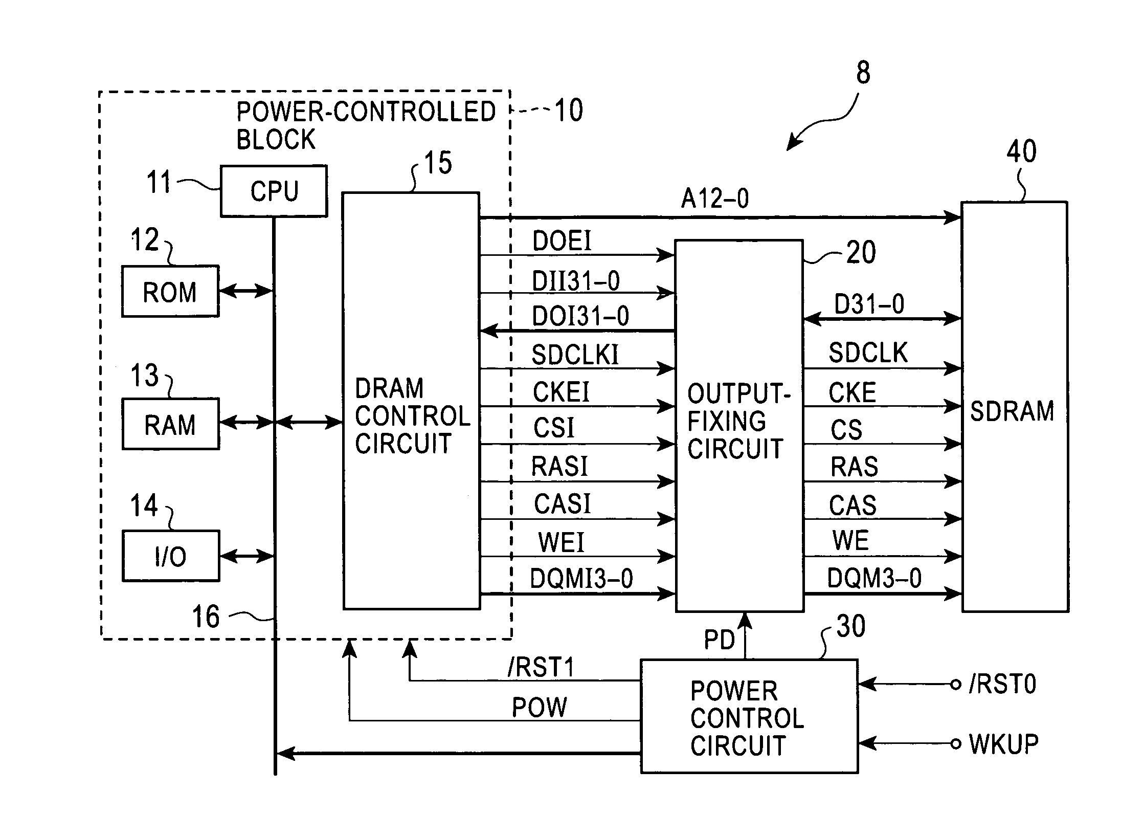
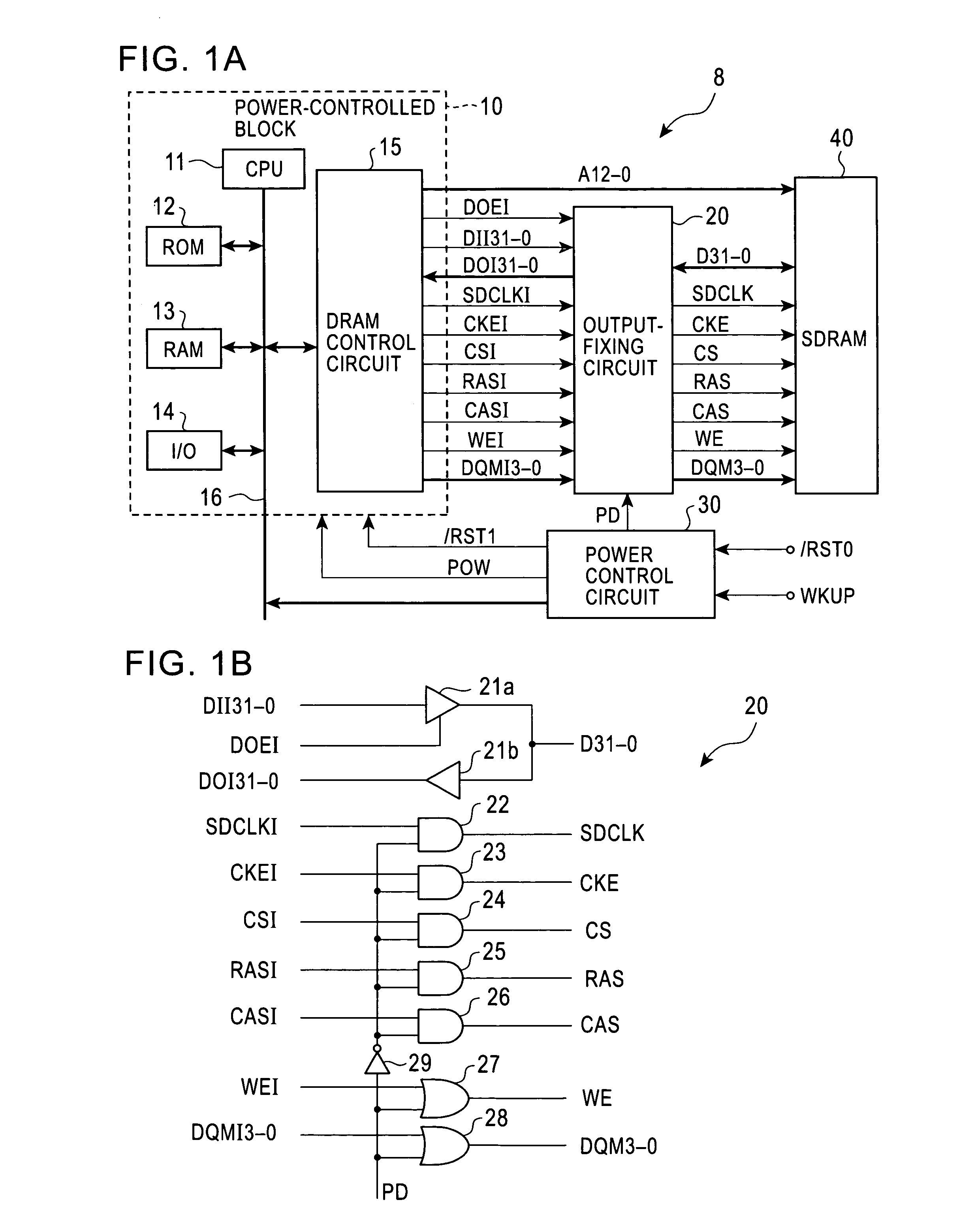
[0014] In the present invention, there are a power control circuit which, when a command to enter the power-saving mode is issued by a CPU, stops the supply of power to the power-controlled block including the CPU after a power-down signal has been generated, and an output-fixing circuit for outputting a control signal to the DRAM upon receiving the power-down signal with the level of the control signal fixed to a level that designates the self-refresh operation. Power supply to the power-controlled block having a broad range of components, including the CPU, the DRAM control circuit, and the like but excluding the power control circuit, the output-fixing circuit, and the DRAM, can thereby be stopped in the power-saving mode, and power consumption can be thoroughly reduced.

Problems solved by technology

With the miniaturization of semiconductor integrated circuits and the increase in the operating frequency in recent years, it has become impossible to ignore the off-leak current of transistors in the CPU and other components, and the ratio of current consumption during inactivity with respect to overall current consumption has increased.
For this reason, it is impossible to adequately reduce power consumption of the system LSI by simply reducing the current consumption during operation with the conventional approaches, i.e., stopping the clock and optimizing the operating frequency.

Method used


Image

  • Semiconductor integrated circuit and power-saving control method thereof
  • Semiconductor integrated circuit and power-saving control method thereof
  • Semiconductor integrated circuit and power-saving control method thereof

Examples


Embodiment Construction

[0021] Referring to FIG. 1A and FIG. 1B, a semiconductor integrated circuit 8 according to an embodiment of the present invention will be described.

[0022] As shown in FIG. 1A, the semiconductor integrated circuit 8 has a power-controlled block 10 that is designed to be powered off in the power-saving mode, an output-fixing circuit 20 that is not designed be powered off, a power control circuit 30 that is not designed be powered off, and an SDRAM (Synchronous DRAM) 40 that is not designed be powered off. The SDRAM 40 is connected to the output-fixing circuit 20. Because the stored content would be lost if the power is shut off, the SDRAM 40 is not designed to be powered off. However, the SDRAM 40 is able to retain the stored content with low power by specifying a self-refresh operation when reading and writing access is not required.

[0023] Included in the power-controlled block 10 are a CPU 11 that controls the entire system and performs computational routines, a ROM 12 in which pr...


PUM


Abstract

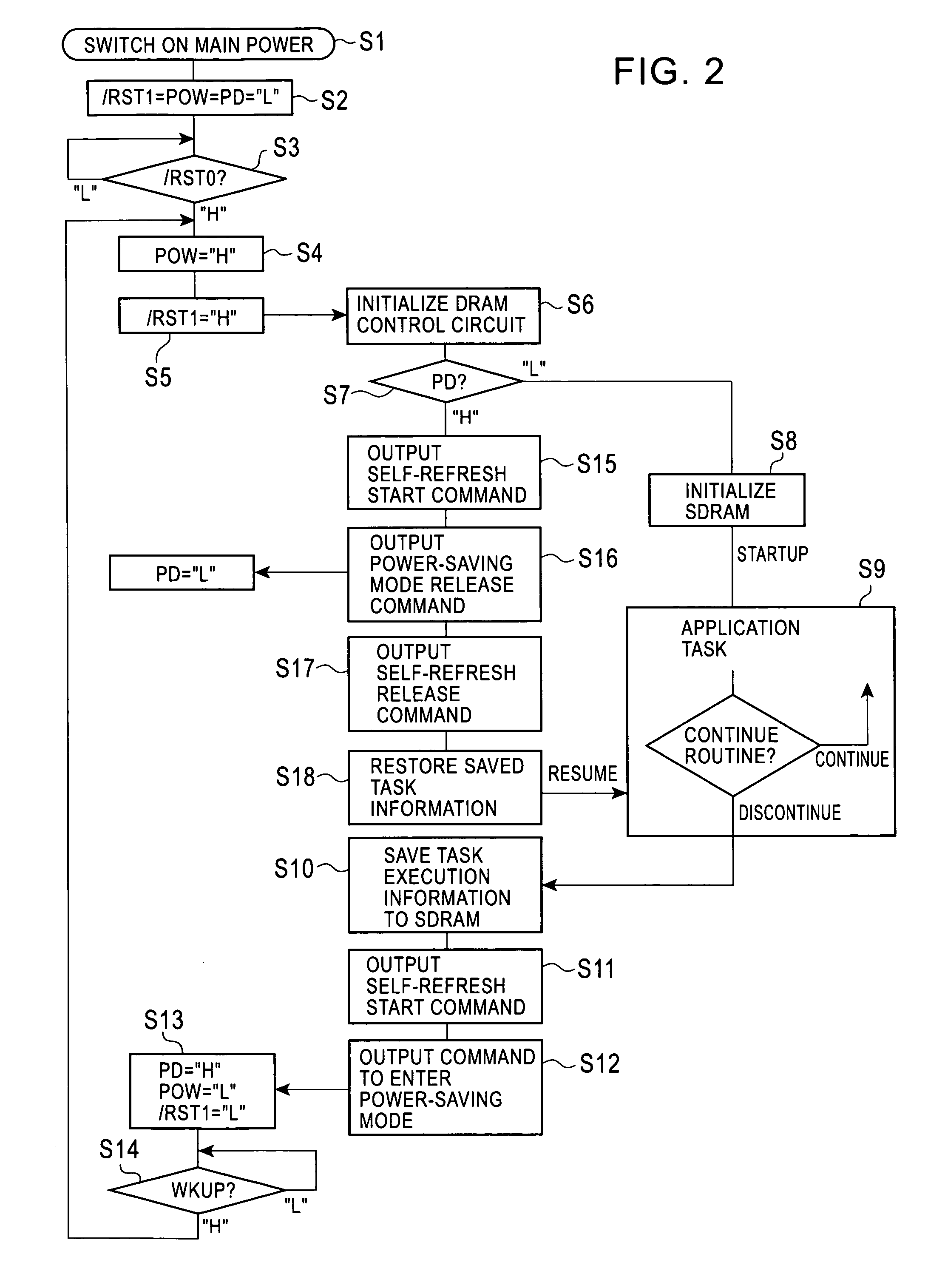
A semiconductor integrated circuit has an SDRAM and a group of elements, whose power consumption is controlled (referred to as “power-controlled block”). The power-controlled block includes a CPU and a memory control circuit. A power control circuit outputs a power-down signal to an output-fixing circuit when a power-saving mode setting command is supplied from the CPU. A control signal for commanding self-refresh operation is generated from the output-fixing circuit to the SDRAM. The power control circuit thereafter stops the supply of power to the entire power-controlled block in response to a power control signal. When a restart signal is provided, the power control circuit starts the supply of power to the power-controlled block. A power-saving mode release command is then generated from the CPU to the power control circuit, and the power-down signal is stopped. Thereupon, the output-fixing circuit provides a control signal generated from the memory control circuit directly to the SDRAM.

Description

BACKGROUND OF THE INVENTION [0001] 1. Field of the Invention [0002] The present invention relates to a semiconductor integrated circuit having a DRAM (Dynamic Random Access Memory) and power-saving control method thereof. [0003] 2. Description of the Related Art [0004] A semiconductor integrated circuit and power-saving control method are known in the art, and examples are disclosed in Japanese Patent Kokai (Laid-open Application) Nos. 2001-357672 and 2003-131935. [0005] A system LSI (Large Scale Integration) is usually provided with a CPU (Central Processing Unit) for carrying out computational routines and controlling the entire system on the basis of a program, a ROM (Read Only Memory) in which programs and other fixed information are stored, a small-capacity RAM (Random Access Memory) for high-speed writing in the stack area and other locations of the OS (Operating System), a large capacity DRAM for storing application programs and intermediate processing data, and I / O (Input / Ou...

Claims


Application Information

Patent Timeline
IPC IPC(8): G06F1/32G06F12/00G06F12/14
CPCG06F1/3203Y02B60/1228Y02B60/32G06F1/3275Y02D10/00Y02D30/50G06F12/00G11C11/407
Inventor ISHIHARA, YUZO
Owner OKI ELECTRIC IND CO LTD
Learn More