Photovoltaic cell, photovoltaic cell module, method of fabricating photovoltaic cell and method of repairing photovoltaic cell

a photovoltaic cell and photovoltaic cell technology, applied in the field of photovoltaic cell, photovoltaic cell module, method of fabricating photovoltaic cell and method of repairing photovoltaic cell, can solve the problems of reverse bias repair, reverse bias repair is not applicable to and the short-circuited portion of the photovoltaic conversion module cannot be recovered with tandem photovoltaic conversion cells

Inactive Publication Date: 2005-12-29
SANYO ELECTRIC CO LTD
View PDF4 Cites 94 Cited by
  • Summary
  • Abstract
  • Description
  • Claims
  • Application Information

AI Technical Summary

Benefits of technology

[0015] An object of the present invention is to provide a tandem photovoltaic cell that is prevented from generation of a short-circuited portion during fabrication, and whose short-circuited portion can be recovered by applying a reverse bias voltage, and provide a photovoltaic cell module comprising such tandem photovoltaic cells and a method of fabricating such tandem photovoltaic cells.

Problems solved by technology

The present inventors, however, found that such a thin film photovoltaic conversion module with an intermediate reflective layer has following problems occurring during the formation of separation grooves by etching.
The above-described reverse bias repair, however, is not applicable to tandem photovoltaic conversion cells, because of the reasons as described below.
For this reason, the reverse bias repair is not applicable to tandem photovoltaic conversion cells.
It has therefore been difficult to recover short-circuited portions in photovoltaic conversion modules with tandem photovoltaic conversion cells.

Method used


Image

  • Photovoltaic cell, photovoltaic cell module, method of fabricating photovoltaic cell and method of repairing photovoltaic cell
  • Photovoltaic cell, photovoltaic cell module, method of fabricating photovoltaic cell and method of repairing photovoltaic cell
  • Photovoltaic cell, photovoltaic cell module, method of fabricating photovoltaic cell and method of repairing photovoltaic cell

Examples


first embodiment

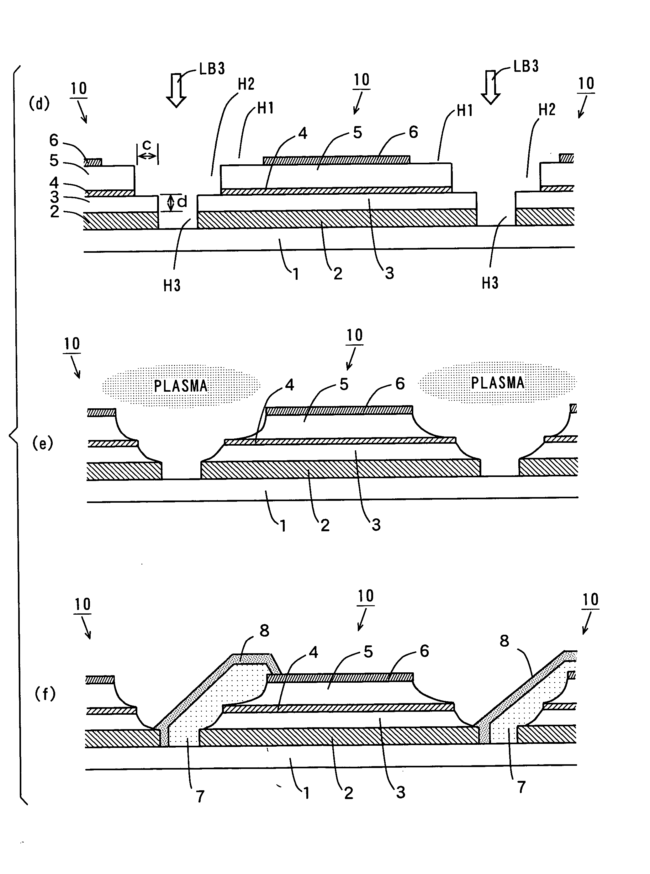
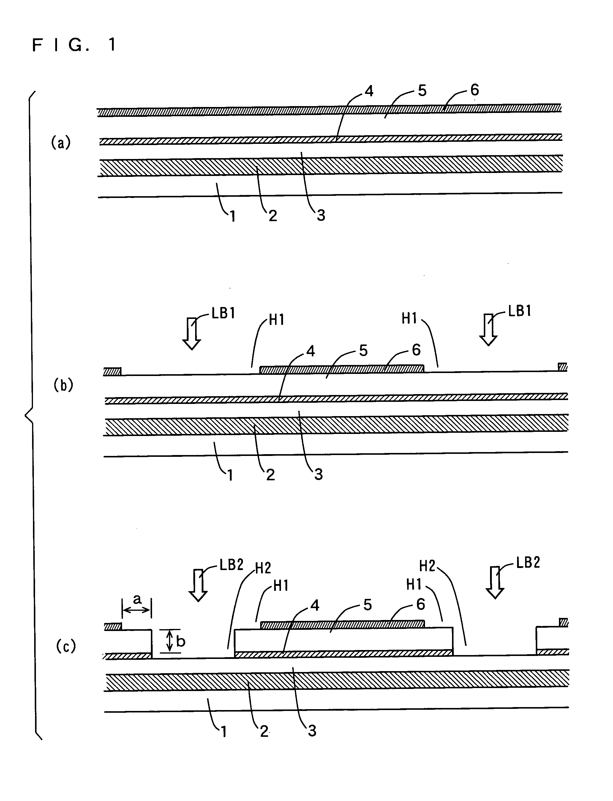
[0085] FIGS. 1(a ), 1(b ), 1(c ) and FIGS. 2(d), 2(e), 2(f) are schematic cross sections showing the steps of a method for fabricating a tandem photovoltaic cell module according to a first embodiment of the invention.

[0086] First, as shown in FIG. 1(a ), a light receptive electrode 2, a first photovoltaic conversion layer 3, an intermediate reflective layer 4, a second photovoltaic conversion layer 5, and a back electrode 6 are formed in order on a transparent substrate 1.

[0087] The transparent substrate 1 may be made of a glass plate, a transparent resin film, or other suitable materials. The light receptive electrode 2 is made of a transparent conductive oxide such as ITO (indium-tin oxide), for example. The first photovoltaic conversion layer 3 has a structure that includes, from the light receptive electrode 2 side, a p-type amorphous silicon layer, an i-type amorphous silicon layer, and an n-type amorphous silicon layer.

[0088] The intermediate reflective layer 4 is made of ...

second embodiment

[0107] FIGS. 6(a ), 6(b ), 6(c ) and FIGS. 7(d), 7(e), 7(f) are schematic cross sections showing the steps of a method for fabricating a tandem photovoltaic cell module according to a second embodiment of the invention.

[0108] First, as shown in FIG. 6(a ), a back electrode 22, a first photovoltaic conversion layer 23, an intermediate reflective layer 24, a second photovoltaic conversion layer 25, and a light receptive electrode 26 are formed in order on a substrate 21.

[0109] The substrate 21 may be made, for example, of a thin plate of stainless onto which PES (polyethersulfone), PI (polyimide), or the like is adhered. The back electrode 22 is made of a laminated film, for example, of a metal material such as silver, aluminum, titanium, and copper, and a metal oxide such as ZnO, ITO, and SnO2. The first photovoltaic conversion layer 23 has a structure that includes, from the back electrode 22 side, an n-type crystalline silicon layer, an i-type crystalline silicon layer, and a p-t...

examples

[0130] In Examples, photovoltaic cell modules were fabricated as follows according to the procedure shown in FIG. 6 and FIG. 7.

[0131] A 0.2-mm thin plate of stainless to which PES was adhered was used as a substrate 21. A laminated film of 200-nm silver and 100-nm ZnO was used as a back electrode 22. A 3-μm crystalline silicon layer that includes, from the substrate 21 side, an n-type microcrystalline silicon layer, an i-type microcrystalline silicon layer, and a p-type microcrystalline silicon layer was used as a first photovoltaic conversion layer 23. ZnO with a thickness of 40 nm was used as an intermediate reflective layer 24. A 300-nm amorphous silicon layer that includes, from the intermediate reflective layer 24 side, an n-type amorphous silicon layer, an i-type amorphous silicon layer, and a p-type amorphous silicon layer was used as a second photovoltaic conversion layer 25. ITO with a thickness of 75-nm was used as a light reflective electrode 26.

[0132] The third harmoni...


PUM


Abstract

A plurality of first separation grooves are formed in a back electrode. Second separation grooves having a width smaller than that of the first separation grooves are formed by removing a second photovoltaic conversion layer and an intermediate reflective layer inside the first separation grooves. Third separation grooves having a width smaller than that of the second separation grooves are formed by removing a first photovoltaic conversion layer and a light reflective electrode inside the second separation grooves. Corners of the first photovoltaic conversion layer and corners of the second photovoltaic conversion layer that are exposed in the separation grooves are removed by performing plasma etching, so that the upper surfaces of side ends of the intermediate reflective layer are exposed.

Description

BACKGROUND OF THE INVENTION [0001] 1. Field of the Invention [0002] The present invention relates to tandem photovoltaic cells, photovoltaic cell modules comprising the tandem photovoltaic cells, a method of fabricating the tandem photovoltaic cells, and a method of repairing the tandem photovoltaic cells. [0003] 2. Description of the Background Art [0004] Tandem photovoltaic cells have been developed for enhancing the photovoltaic conversion efficiency. FIG. 12 is a cross section showing an example of a thin film photovoltaic conversion module that includes conventional tandem photovoltaic conversion cells (refer to JP 2002-261308 A, for example). The thin film photovoltaic conversion module shown in FIG. 12 has a plurality of photovoltaic conversion cells 120. Each photovoltaic conversion cell 120 has a tandem structure that includes a transparent front electrode layer 122, an amorphous photovoltaic conversion layer 123, an intermediate reflective layer 124, a crystalline photovol...

Claims


Application Information

Patent Timeline
Patent Type & Authority Applications(United States)
IPC IPC(8): H01L21/00H01L25/00H01L27/142H01L31/00H01L31/0463H01L31/0465H01L31/052H01L31/056H01L31/06H01L31/075H01L31/076H01L31/18
CPCH01L31/076Y02E10/52H01L31/0547H01L31/0475Y02E10/548
Inventor SHINOHARA, WATARU
Owner SANYO ELECTRIC CO LTD
Why Eureka
Try Eureka