Organic TFT and method of fabricating the same

a thin film transistor and organic technology, applied in the field of thin film transistors, can solve the problems of high leakage current, increased driving voltage of the device to which the tft is applied, and pin holes in the insulation, and achieve the effect of low threshold voltage and low leakage curren

Active Publication Date: 2005-12-29
SAMSUNG DISPLAY CO LTD
View PDF19 Cites 63 Cited by
  • Summary
  • Abstract
  • Description
  • Claims
  • Application Information

AI Technical Summary

Benefits of technology

[0009] The present invention provides a TFT that has an organic gate insulator that allows the TFT to have flexibility, a low threshold voltage, and a low leakage current.

Problems solved by technology

However, the organic gate insulator may incur a pin hole during its formation, and have a high leakage current due to the weakness of the material itself.
This may cause an increase in a driving voltage of a device to which the TFT is applied.

Method used


Image

  • Organic TFT and method of fabricating the same
  • Organic TFT and method of fabricating the same
  • Organic TFT and method of fabricating the same

Examples


Embodiment Construction

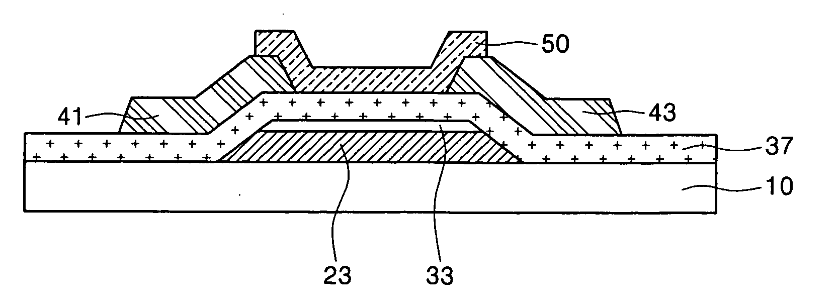
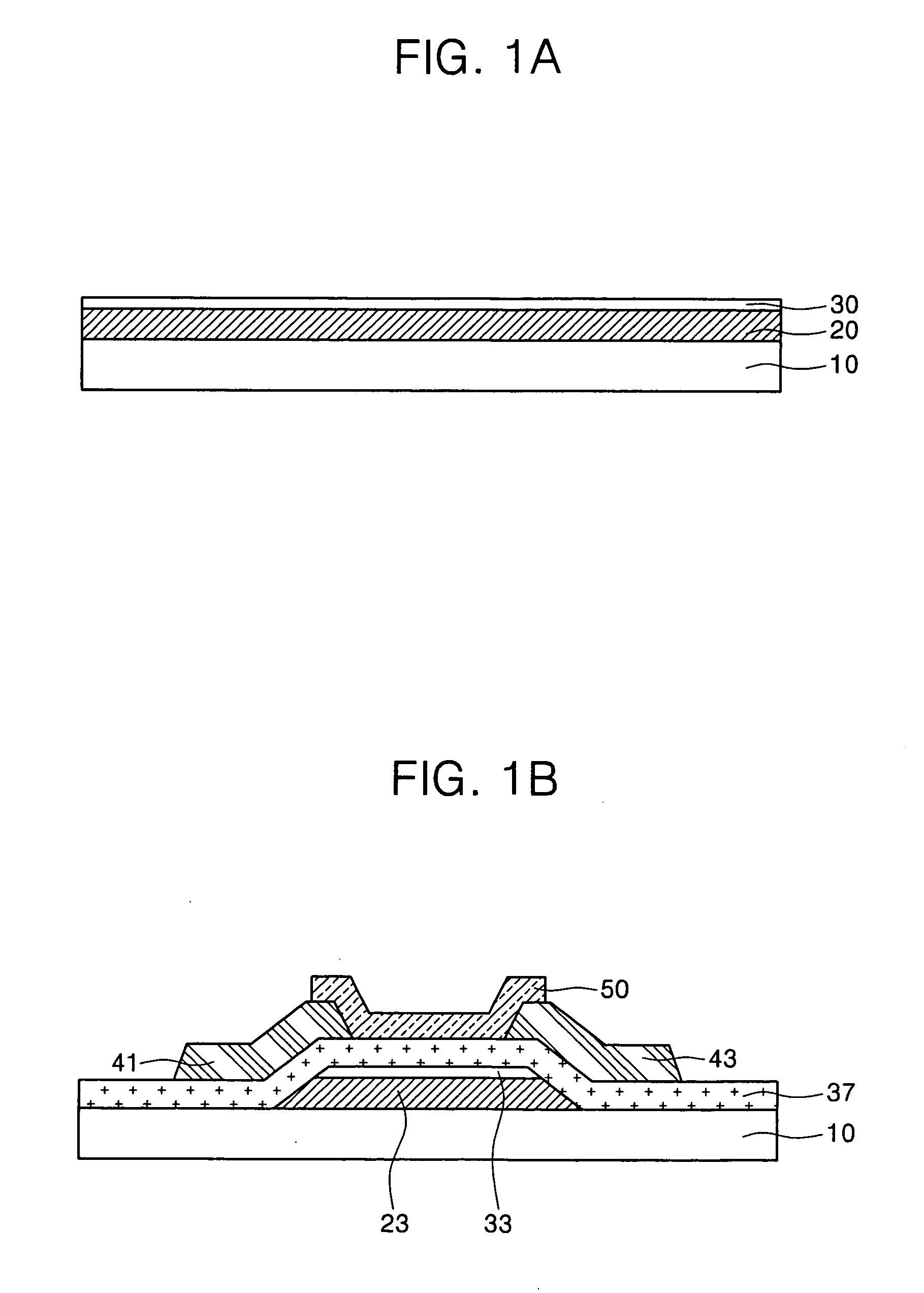
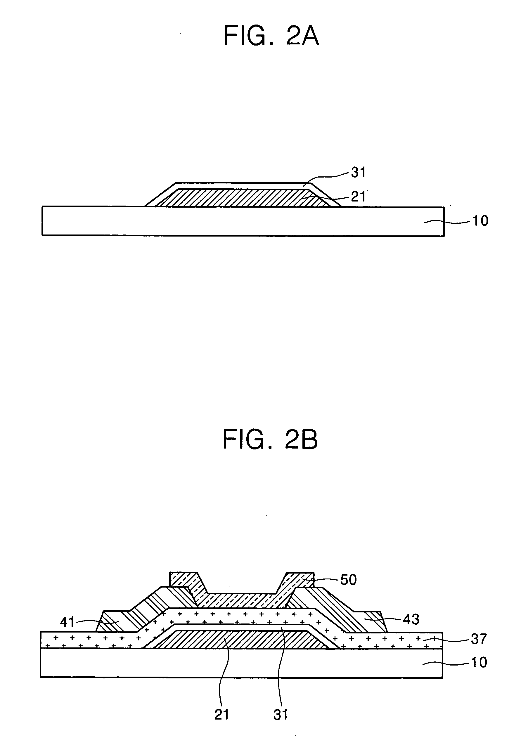
[0023]FIG. 1A and FIG. 1B are cross-sectional views that illustrate process steps in a method for fabricating an OTFT in accordance with an exemplary embodiment of the present invention.

[0024] Referring to FIG. 1A, a substrate 10 is prepared. The substrate 10 may be made of glass, plastic, sapphire, or quartz, for example. Preferably, the substrate 10 is a flexible material such as a plastic.

[0025] A gate conductive layer 20 is formed on the substrate 10. The gate conductive layer 20 may be formed of Ta, W, Ti, Mo, Al, Au, Cu, Y, Zn, Hf, Zr, or an alloy thereof, for example. The alloy may be one of MoW, AlNd, AlCu, AuTi, and AuCr. Alternatively, the gate conductive layer 20 may comprise doped silicon or a conductive organic material.

[0026] A barrier layer (not shown) may be formed on the substrate 10 prior to the formation of the gate conductive layer 20. The barrier layer protects a subsequently formed organic semiconductor layer from moisture or an organic gas that may be intro...


PUM


Abstract

The present invention provides an organic thin film transistor and method for fabricating the same. The organic thin film transistor has a substrate and a gate electrode that is positioned on the substrate. A gate insulator has a stacked structure comprising an inorganic gate insulator and an organic gate insulator that are positioned on the gate electrode. An organic semiconductor layer is positioned on the gate insulator to overlap the gate electrode. Accordingly, an organic thin film transistor that has flexibility, decreased leakage current, and a low threshold is formed.

Description

CROSS-REFERENCE TO RELATED APPLICATION [0001] This application claims priority to and the benefit of Korean Patent Application No. 2004-47892, filed Jun. 24, 2004, the disclosure of which is incorporated by reference in its entirety. BACKGROUND OF THE INVENTION [0002] 1. Field of the Invention [0003] The present invention relates to a thin film transistor (TFT). In particular, the present invention relates to an organic TFT including an organic semiconductor layer and a method for fabricating the same. [0004] 2. Description of the Related Art [0005] In general, a thin film transistor (TFT) includes a semiconductor layer, a gate electrode, a source electrode, and a drain electrode. The semiconductor layer may be formed of a polysilicon layer or an amorphous silicon layer. However, organic compounds such as polyacethylene, which is a conjugated organic polymer, have been studied in recent years. Polyacethylene may have semiconductive properties when it is subjected to doping. Organic ...

Claims


Application Information

Patent Timeline
Patent Type & Authority Applications(United States)
IPC IPC(8): H01L21/00H01L29/08H01L21/786H01L51/05
CPCH01L51/0529H10K10/474H01L21/786
Inventor KOO, JAE-BONSUH, MIN-CHULMO, YEON-GON
Owner SAMSUNG DISPLAY CO LTD
Why Eureka
Try Eureka