Semiconductor device including a multi-channel fin field effect transistor and method of fabricating the same

a technology of fin field effect transistor and semiconductor device, which is applied in the direction of semiconductor devices, electrical devices, transistors, etc., can solve the problems of degrading the characteristics of the device as an active switch, the inability to effectively suppress the influence of the inability to effectively suppress the drain electrical potential on the source electrical potential and the channel, etc., to achieve the effect of increasing the current level of the transistor, increasing the effective channel length of the transistor

Active Publication Date: 2005-12-29
SAMSUNG ELECTRONICS CO LTD
View PDF5 Cites 87 Cited by
  • Summary
  • Abstract
  • Description
  • Claims
  • Application Information

AI Technical Summary

Benefits of technology

[0013] It is yet another feature of an embodiment of the present invention to provide a semiconductor device including a multi-channel FinFET and a method of fabricating the same that significantly increases an effective channel length of the transistor.
[0014] It is still another feature of an embodiment of the present invention to provide a semiconductor device including a multi-channel FinFET and a method of fabricating the same that is able to increase a current lev...

Problems solved by technology

This decrease in channel length, however, may degrade characteristics of the device as an active switch.
Thus, it becomes difficult to effectively suppress an influence of a drain electrical potential on a source electrical potential and a channel electrical potential.
However, since a conventional MOSFET, in which a channel is disposed parallel on a surface of a semiconductor, is a planar channel device, it is difficult to not only structurally scale down the MOSFET, but also to suppress the occurrence of the short channel effect.
Although the FinFET offers these superio...

Method used


Image

  • Semiconductor device including a multi-channel fin field effect transistor and method of fabricating the same
  • Semiconductor device including a multi-channel fin field effect transistor and method of fabricating the same
  • Semiconductor device including a multi-channel fin field effect transistor and method of fabricating the same

Examples


first through fourth embodiments

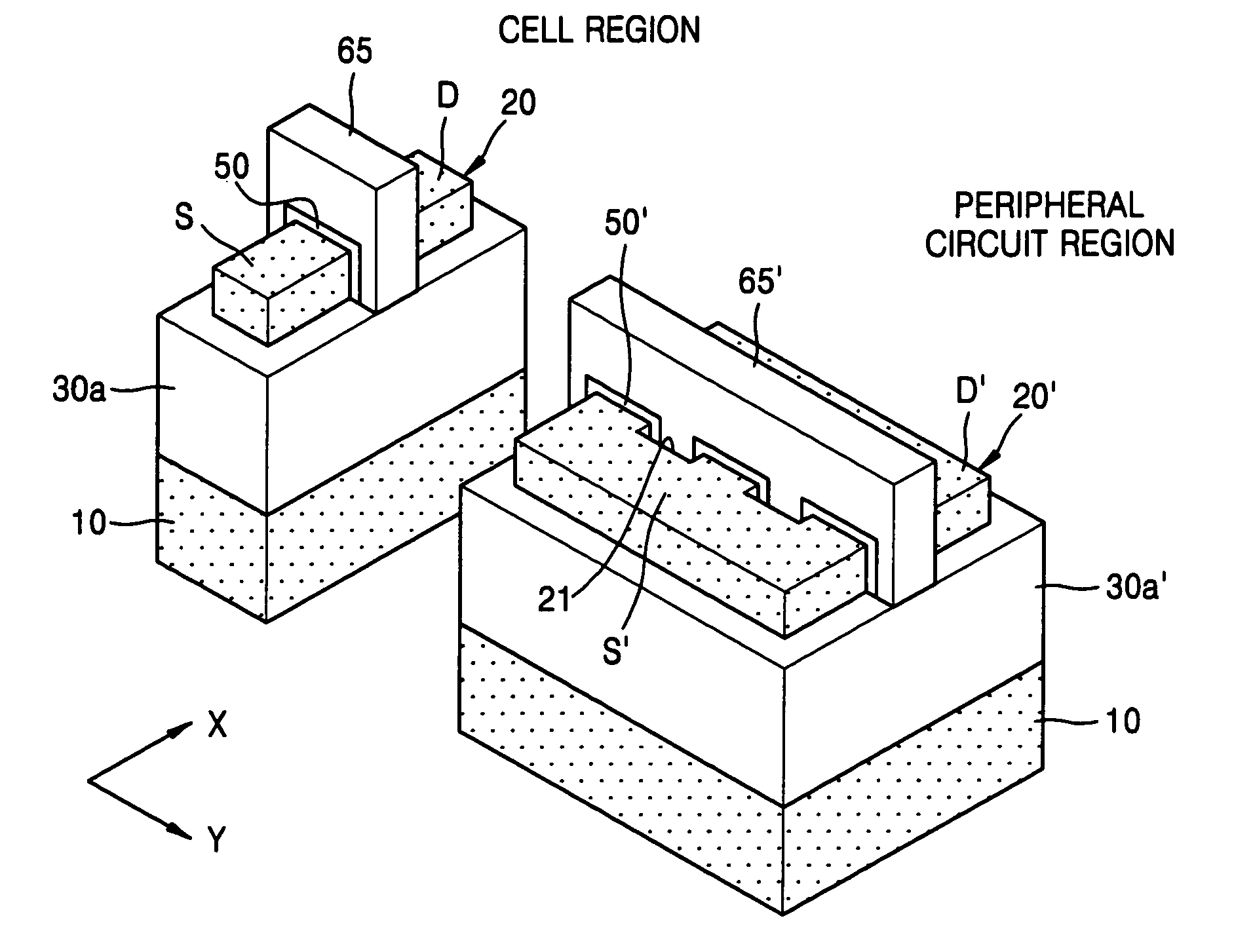
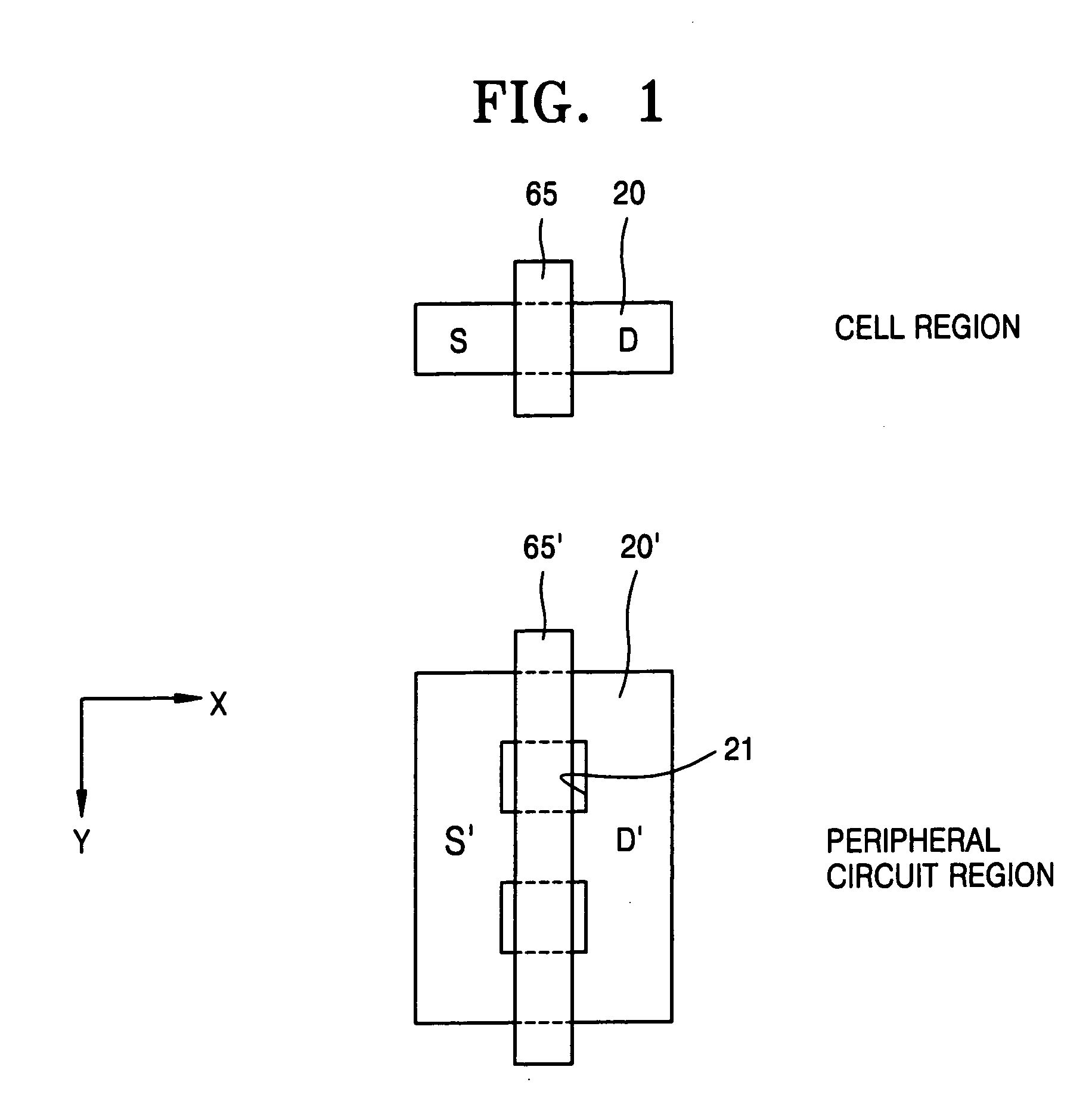
[0047]FIG. 1 illustrates a plan view of a semiconductor device formed by a method of fabricating a semiconductor device according to a first through fourth embodiment of the present invention.

[0048] Referring to FIG. 1, a semiconductor device is divided into a cell region and a peripheral circuit region. The cell region includes an active region 20 and a gate electrode 65. The active region 20 and the gate electrode 65, which is formed on the active region 20, are perpendicular relative to one another. For example, a length of the active region 20 may extend in an x-direction and a length of the gate electrode 65 may extend in a y-direction. The active region 20 includes a source S and a drain D formed on either side of the gate electrode 65.

[0049] The peripheral circuit region includes an active region 20′ and a gate electrode 65′, which is formed on the active region 20′. The active region 20′ and the gate electrode 65′ are both substantially rectangular in shape. A length of th...

fifth and sixth embodiments

[0116]FIG. 20 illustrates a plan view of a semiconductor device formed by a method of fabricating a semiconductor device according to a fifth and a sixth embodiment of the present invention.

[0117] Referring to FIG. 20, the semiconductor device is divided into a cell region and a peripheral circuit region. The cell region includes an active region 120 and a gate electrode 165. The active region 120 and the gate electrode 165, which is formed on the active region 120, are perpendicular relative to one another. For example, a length of the active region 120 may extend in an x-direction and a length of the gate electrode 165 may extend in a y-direction. The active region 120 includes a source S and a drain D formed on either side of the gate electrode 165.

[0118] The peripheral circuit region includes an active region 120′ and a gate electrode 165′, which is formed on the active region 120′. The active region 120′ and the gate electrode 165′ are both substantially rectangular in shape....


PUM


Abstract

In a semiconductor device, and a method of fabricating the same, the semiconductor device includes a semiconductor substrate having a cell region and a peripheral circuit region, a portion of the semiconductor substrate in the cell region and in the peripheral circuit region including an isolation region defining an active region, a portion of the active region protruding above an upper surface of the isolation region to define at least two active channels, a gate dielectric layer formed over the active region of the semiconductor substrate including the at least two protruding active channels, a gate electrode formed over the gate dielectric layer and the isolation region of the semiconductor substrate, and a source/drain region formed in the active region of the semiconductor substrate on either side of the gate electrode.

Description

BACKGROUND OF THE INVENTION [0001] 1. Field of the Invention [0002] The present invention relates to a semiconductor device including a multi-channel fin field effect transistor (FinFET) and a method of fabricating the same. More particularly, the present invention relates to a semiconductor device including a multi-channel FinFET in a cell and / or peripheral circuit region of a semiconductor substrate and a method of fabricating the same. [0003] 2. Description of the Related Art [0004] In order to improve performance and reduce fabrication cost of semiconductor devices, an integration density of semiconductor devices must continually increase. Increasing integration density of semiconductor devices requires developing techniques for reducing a feature size of a semiconductor device. [0005] In conventional semiconductor fabricating processes, the channel length of a metal-oxide-semiconductor field effect transistor (MOSFET) is decreased to increase an operating speed and integration ...

Claims


Application Information

Patent Timeline
IPC IPC(8): H01L21/336H01L21/84H01L27/12H01L29/78H01L29/786
CPCH01L21/84H01L27/1203H01L29/78684H01L29/66795H01L29/785H01L29/66545H01L21/18
Inventor KIM, SUNGMINPARK, DONGGUNYOON, EUNJUNGJANG, SEMYEONGKIM, KEUNNAMOH, YONGCHUL
Owner SAMSUNG ELECTRONICS CO LTD
Why Eureka
Try Eureka