New fuse structure

Inactive Publication Date: 2005-12-29
TAIWAN SEMICON MFG CO LTD
View PDF18 Cites 70 Cited by
  • Summary
  • Abstract
  • Description
  • Claims
  • Application Information

AI Technical Summary

Benefits of technology

[0012] The vertical structure of the preferred embodiment is suitable to be formed in any layer and saves layout space. The embodiments of the present invention have several advantageous features. Firstly, higher repairable rates can be achieved since the burn out

Problems solved by technology

However, the laser repair rate in various structures such as in lower level metal layers is low and the process is complex. FIG. 1 illustrates a laser fuse formed close to the surface of a chip.
If a laser fuse 10 is in a lower level layer deep in a chip, as shown in FIG. 2, the opening 8 will be deeper, while the thickness T of the oxide still has to be controlled precisely, which increases the complexity significantly and decreases the repairable rate.
This decreases the device reliability and increases

Method used


Image

  • New fuse structure
  • New fuse structure
  • New fuse structure

Examples


Example

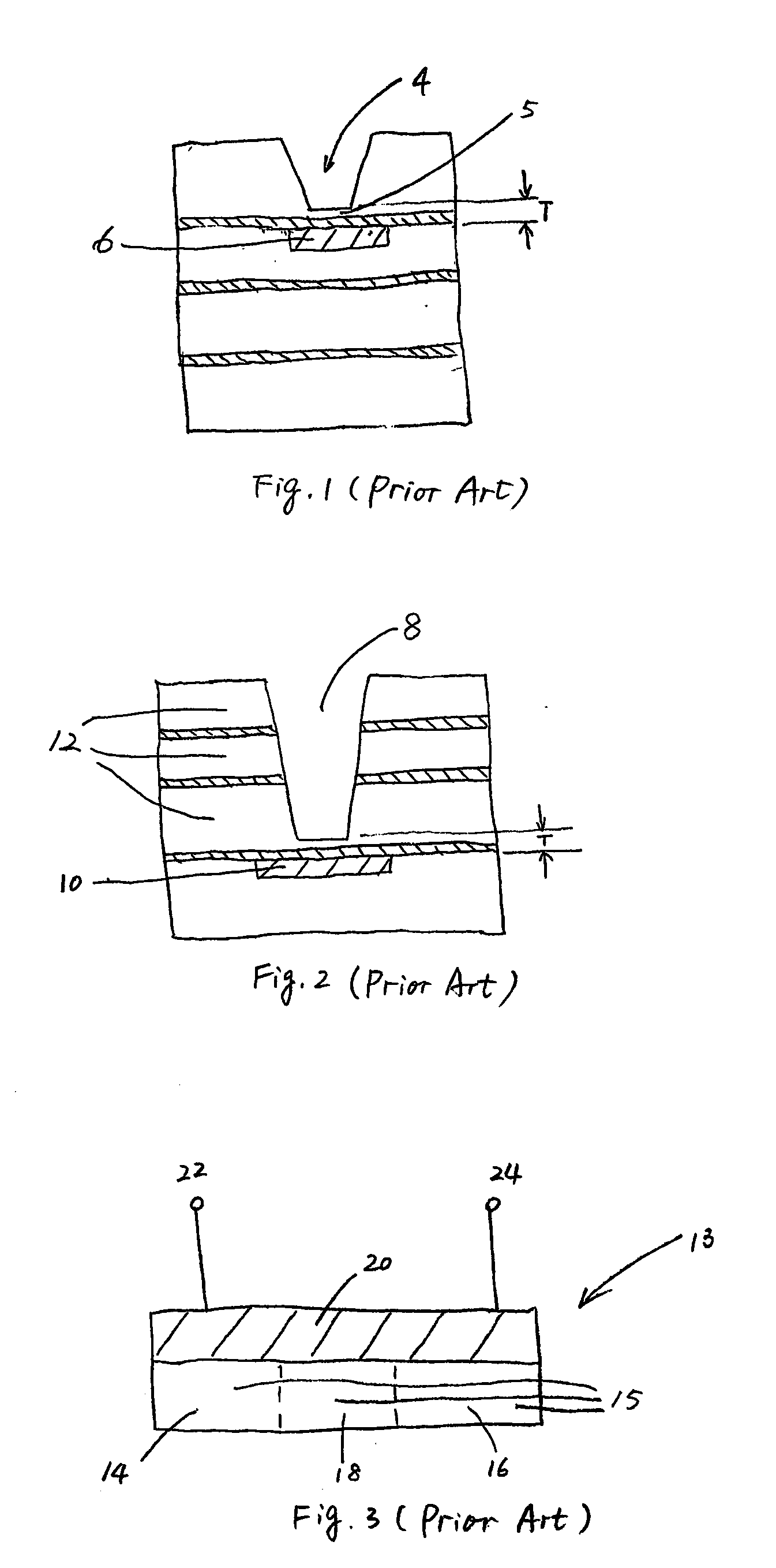
[0024] The making and using of the presently preferred embodiments are discussed in detail below. It should be appreciated, however, that the present invention provides many applicable inventive concepts that can be embodied in a wide variety of specific contexts. The specific embodiments discussed are merely illustrative of specific ways to make and use the invention, and do not limit the scope of the invention.

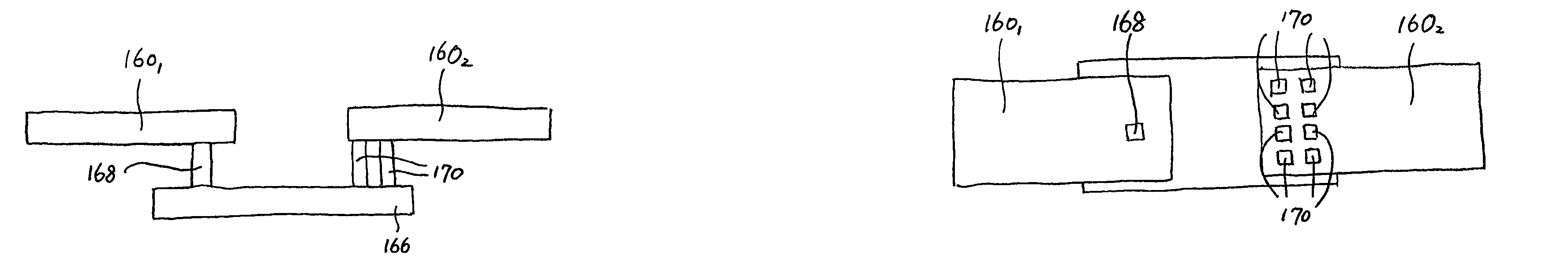
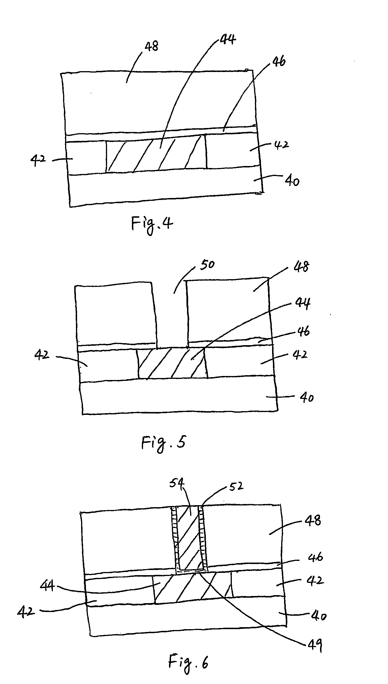
[0025] The preferred embodiments of the present invention present a novel method of forming e-fuses. A via connecting a lower-layer conductive line and an upper-layer conductive line is adapted to be an e-fuse. The e-fuse can be burned out by applying a voltage on external pads that are coupled to the lower-layer conductive line and the upper-layer conductive line. Throughout the description, conductive lines are also referred to as conductive layers.

[0026]FIGS. 4 through 7 are cross-sectional views of intermediate stages in the making of a preferred embodiment of the pres...


PUM


Abstract

An electrical fuse and a method of forming the same are presented. A first-layer conductive line is formed over a base material. A via is formed over the first-layer conductive line. The via preferably comprises a barrier layer and a conductive material. A second-layer conductive line is formed over the via. A first external pad is formed coupling to the first-layer conductive line. A second external pad is formed coupling to the second-layer conductive line. The via, the first conductive line and the second conductive line are adapted to be an electrical fuse. The electrical fuse can be burned out by applying a current. The vertical structure of the preferred embodiment is suitable to be formed in any layer.

Description

[0001] This application claims the benefit of U.S. Provisional Application No. 60 / 583,637, filed on Jun. 29, 2004, entitled “E-Fuse Structure Design in Electrical Programmable Redundancy for Embedded Memory Circuit,” which application is hereby incorporated herein by reference.TECHNICAL FIELD [0002] This invention relates generally to an electrical fuse and more particularly to an electrical fuse having a vertical structure. BACKGROUND [0003] In the semiconductor industry, fuse elements are widely used features in integrated circuits for a variety of purposes, such as improving manufacturing yield or customizing a generic integrated circuit. For example, by replacing defective circuits on a chip with redundant circuits on the same chip, manufacturing yields can be significantly increased. Replacing defective circuits is especially useful for improving manufacturing yield of the memory chips since memory chips consist of a lot of identical memory cells and cell groups. By selectively...

Claims


Application Information

Patent Timeline
IPC IPC(8): H01L23/525H01L23/532H01L29/00
CPCH01L23/5256H01L23/53238H01L23/53295H01L2924/0002H01L2924/00
Inventor THEI, KONG-BENGCHENG, CHUNG LONGLIU, CHUNG-SHICHUANG, HARRYWU, SHIEN-YANGCHEN, SHI-BAI
Owner TAIWAN SEMICON MFG CO LTD
Why Eureka
Try Eureka