Etch and deposition control for plasma implantation

a plasma implantation and control technology, applied in the field of ion implantation for materials processing, can solve the problems of limited throughput, high cost, and complex machine of the typical ion-beam implanter, and achieve the effect of reducing surface damag

Inactive Publication Date: 2005-12-29
VARIAN SEMICON EQUIP ASSOC INC
View PDF22 Cites 32 Cited by
  • Summary
  • Abstract
  • Description
  • Claims
  • Application Information

AI Technical Summary

Benefits of technology

[0012] Accordingly, in a first aspect, the invention features a method for plasma implantation, such as plasma doping, of a substrate. The method includes forming a plasma from one or more implant materials, implanting one or more implant species into a surface of the substrate, and directing one or more surface-modifying species at the surface to reduce surface damage associated with the plasma. An implant material can provide at least one dopant species, and a surface-modifying material can provide one or more surface-modifying species. The substrate can be, for example, immersed in the plasma, or positioned near to the plasma, to provide implantation of species from the plasma, and the plasma can be formed from both the implant materials and the surface-modifying materials.

Problems solved by technology

Unfortunately, however, a typical ion-beam implanter is a complex and costly machine, and can have a limited throughput.
For example, at energies under 10 keV, as can be required for shallow junction formation, wafer throughput can suffer.
Further, unwanted deposition and / or etch can occur as a function of the particular chemistry and operating conditions utilized for a particular implant process, due to exposure of a substrate to the plasma neutrals.
For example, when using BF3 as a dopant gas, plasma components related to fluorine can cause unwanted etching.
The need to control process parameters, however, can limit satisfactory process windows.

Method used


Image

  • Etch and deposition control for plasma implantation
  • Etch and deposition control for plasma implantation
  • Etch and deposition control for plasma implantation

Examples


Embodiment Construction

[0018] This invention is not limited in its application to the details of construction and the arrangement of components set forth in the following description or illustrated in the drawings. The invention is capable of other embodiments and of being practiced or of being carried out in various ways. Also, the phraseology and terminology used herein is for the purpose of description and should not be regarded as limiting. The use of “including,”“comprising,” or “having,”“containing”, “involving”, and variations thereof herein, is meant to encompass the items listed thereafter and equivalents thereof as well as additional items.

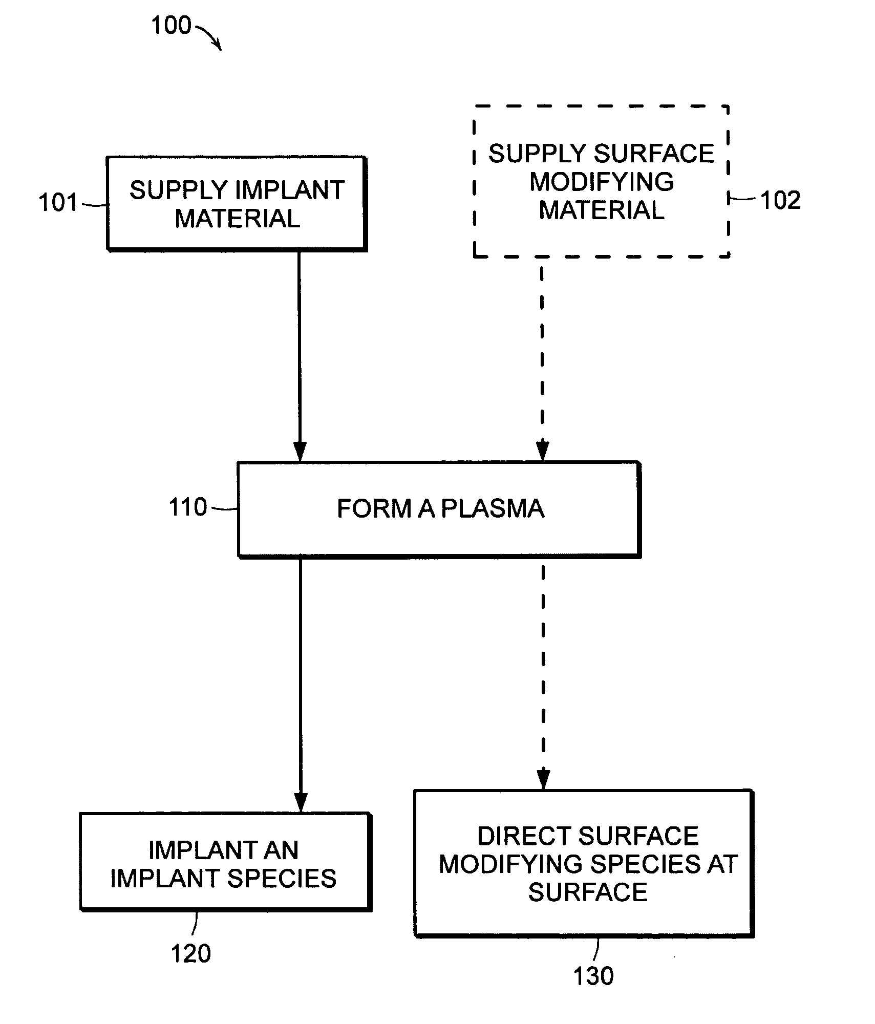
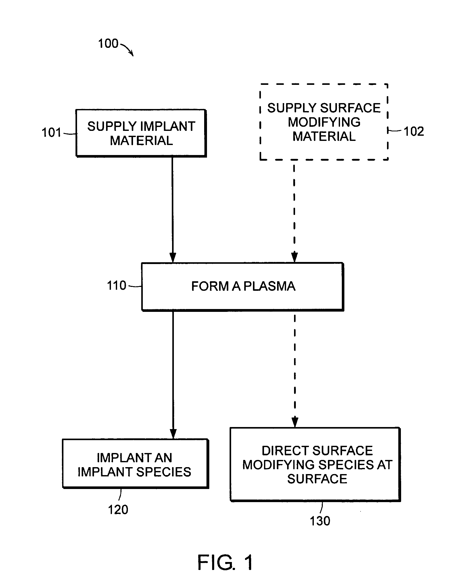
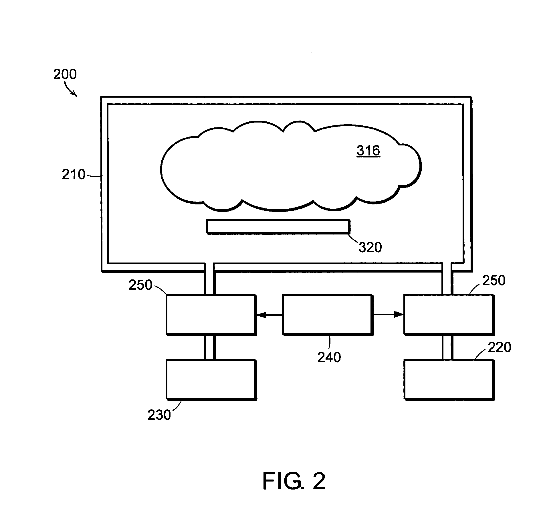
[0019] The word “plasma,” is used herein in a broad sense to refer to a gas-like phase that can include any or all of electrons, atomic or molecular ions, atomic or molecular radical species (i.e., activated neutrals), and neutral atoms and molecules. A plasma typically has a net charge that is approximately zero. A plasma may be formed from one or more mater...


PUM

PropertyMeasurementUnit
pressureaaaaaaaaaa
poweraaaaaaaaaa
timeaaaaaaaaaa

Abstract

A method for ion implantation of a substrate includes forming a plasma from at least one implant material comprising at least one implant species, implanting the at least one implant species into a surface of the substrate, and directing at least one surface-modifying species at the surface to reduce a surface damage associated with the plasma. An apparatus for ion implantation is configured to implement this method.

Description

BACKGROUND OF INVENTION [0001] 1. Field of Invention [0002] The invention is related to ion implantation for materials processing, and, in particular, to methods and apparatus for plasma implantation of dopants for fabrication of semiconductor-based devices. [0003] 2. Discussion of Related Art [0004] The process of adding impurities to a semiconductor to control the semiconductor's electrical properties is known as “doping,” and suitable impurities are known as dopants. Some early doping techniques involved incorporation of dopant either during growth of a substrate, or diffusion of a dopant into a substrate from a gaseous or solid-phase material in contact with the substrate. Diffusion-based techniques involve elevated temperatures to obtain satisfactory dopant diffusion rates in the substrate. [0005] Ion-implantation technology was developed in response to a demand for more precise control over spatial uniformity and concentration of dopants. A typical ion implanter ionizes a dopa...

Claims


Application Information

Patent Timeline
Patent Type & Authority Applications(United States)
IPC IPC(8): C03C15/00C23C14/00H01L21/223
CPCH01J37/32412H01L21/2236
Inventor SINGH, VIKRAMPERSING, HAROLDMILLER, TIMOTHYGUPTA, ATULFANG, ZIWEI
Owner VARIAN SEMICON EQUIP ASSOC INC
Why Eureka
Try Eureka