

Method of fabricating semiconductor device
- Summary
- Abstract
- Description
- Claims
- Application Information
AI Technical Summary
Benefits of technology
Problems solved by technology
Method used
Image

Examples
embodiment 1
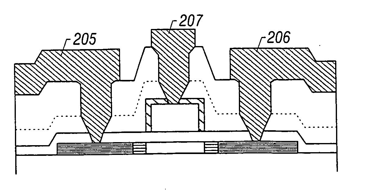
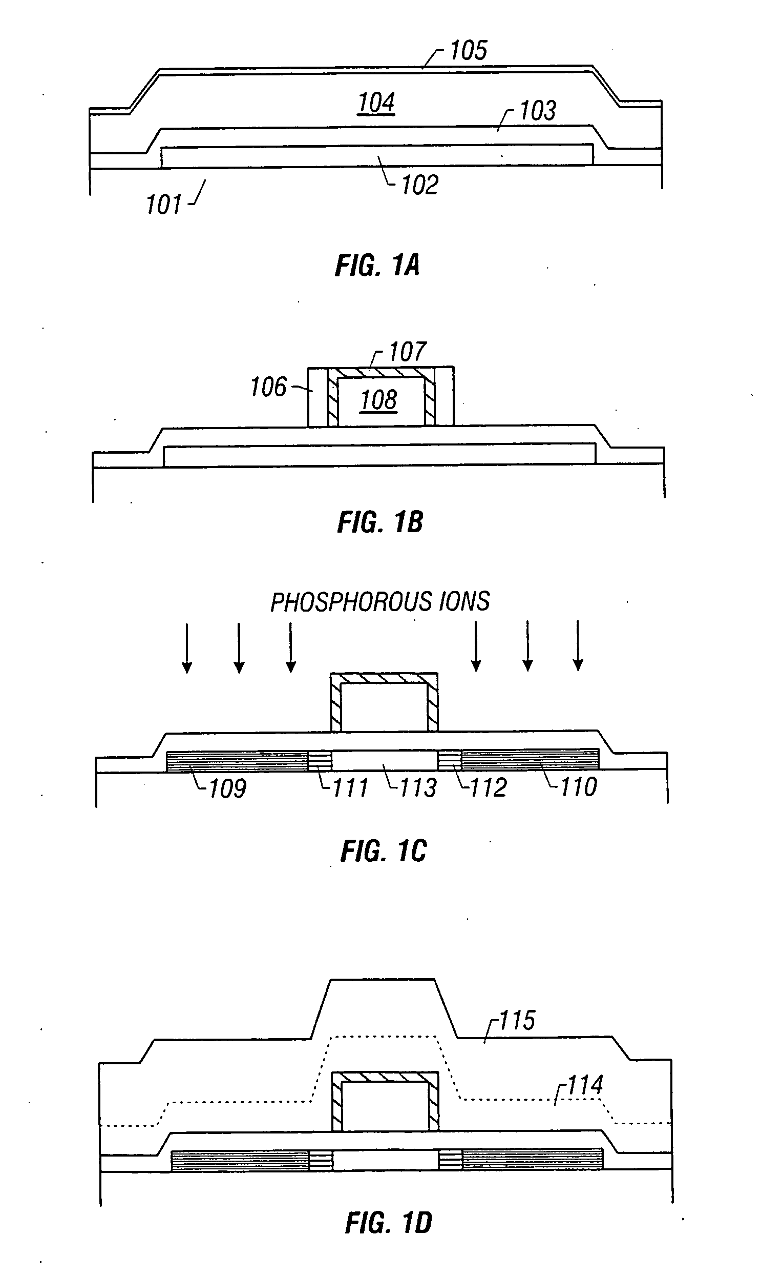
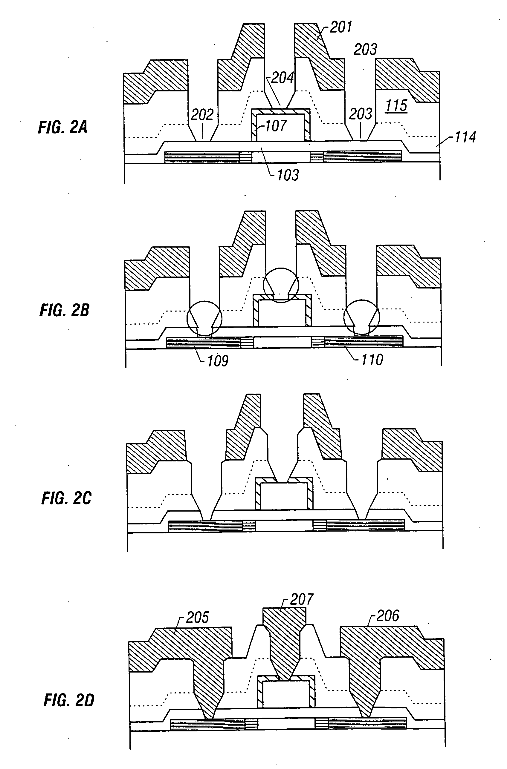
[0040] A process sequence for fabricating TFTs in accordance with the present invention is illustrated in FIGS. 1(A)-1(D) and FIG. 2(A)-2(D).
[0041] First, a glass substrate 101 having an insulating film such as a silicon oxide film on its surface is prepared. An amorphous silicon film (not shown) having a thickness of 500 Å is formed on the substrate by plasma CVD or LP thermal chemical vapor deposition. The amorphous film is crystallized by an appropriate crystallization method, which may be either heating or laser illumination.
[0042] Then, the crystalline silicon film obtained by crystallizing the amorphous silicon film is patterned into islands of a semiconductor layer 102 forming an active layer.
[0043] A silicon oxide film 103 which will act as a gate-insulating film later is formed on the semiconductor layer to a thickness of 1200 Å by plasma CVD or LP thermal chemical vapor deposition.
[0044] Then, a film 104 consisting only or mainly of aluminum is formed to a thickness of...
embodiment 2
[0083] The present example is an example of application of the present invention to an IC fabrication process using single-crystal silicon wafer.
[0084] More specifically, this is an example of fabrication of a MOS transistor, using the silicon wafer.
[0085] The process sequence of the present invention is shown in FIGS. 6(A)-6(C), 7(A)-7(B), and 8(A)-8(B). First, as shown in FIG. 6(A), a thermal oxide film and a silicon nitride film are laminated over an N-type single-crystal silicon wafer 601 and patterned to create a patterned lamination of the thermal oxide film 602 and silicon nitride film 603.
[0086] Then, field oxide films 604 and 605 are formed by a selective thermal oxidization method. Thus, a state shown in FIG. 6(A) is obtained.
[0087] Then, the thermal oxide film 602 and the silicon nitride film 603 are removed. A thermal oxide film 606 is formed again by thermal oxidation. This thermal oxide film 606 forms a gate-insulating film.
[0088] Thereafter, a gate electrode 607 ...
PUM
 Abstract
Description
Claims
Application Information