Semiconductor device improving error correction processing rate

a technology of mikro-conductor and error correction, which is applied in the direction of digital storage, instruments, coding, etc., can solve the problems of critical problem, hardware failure caused by bit errors, data stored in memory cell storage nodes, etc., and achieve the effect of improving the error correction processing ra

Active Publication Date: 2005-12-29
RENESAS ELECTRONICS CORP
View PDF14 Cites 24 Cited by
  • Summary
  • Abstract
  • Description
  • Claims
  • Application Information

AI Technical Summary

Benefits of technology

[0014] In view of the foregoing, an object of the present invention is to provide a semiconductor device further improving the error correction processing rate.

Problems solved by technology

In semiconductor devices such as semiconductor memory devices, bit errors caused by hardware failure are encountered.
There is also known a phenomenon called “soft error”, caused by the generation of pairs of electrons and holes in the silicon substrate when radiation such as α rays and neutron rays present in nature is introduced into the chip, leading to the possibility of destroying, in the worst case, data stored in the storage node of a memory cell.
The bit error caused by such soft error has become a critical problem.
Increase in the number of stages of XOR gates induces the problem that the error correction processing rate will become slower.
The circuit complexity is increased in accordance with the increase in the number of XOR gates, whereby the wiring that connects respective circuits becomes longer.
As a result, the rate of error correction processing is degraded.

Method used


Image

  • Semiconductor device improving error correction processing rate
  • Semiconductor device improving error correction processing rate
  • Semiconductor device improving error correction processing rate

Examples


first embodiment

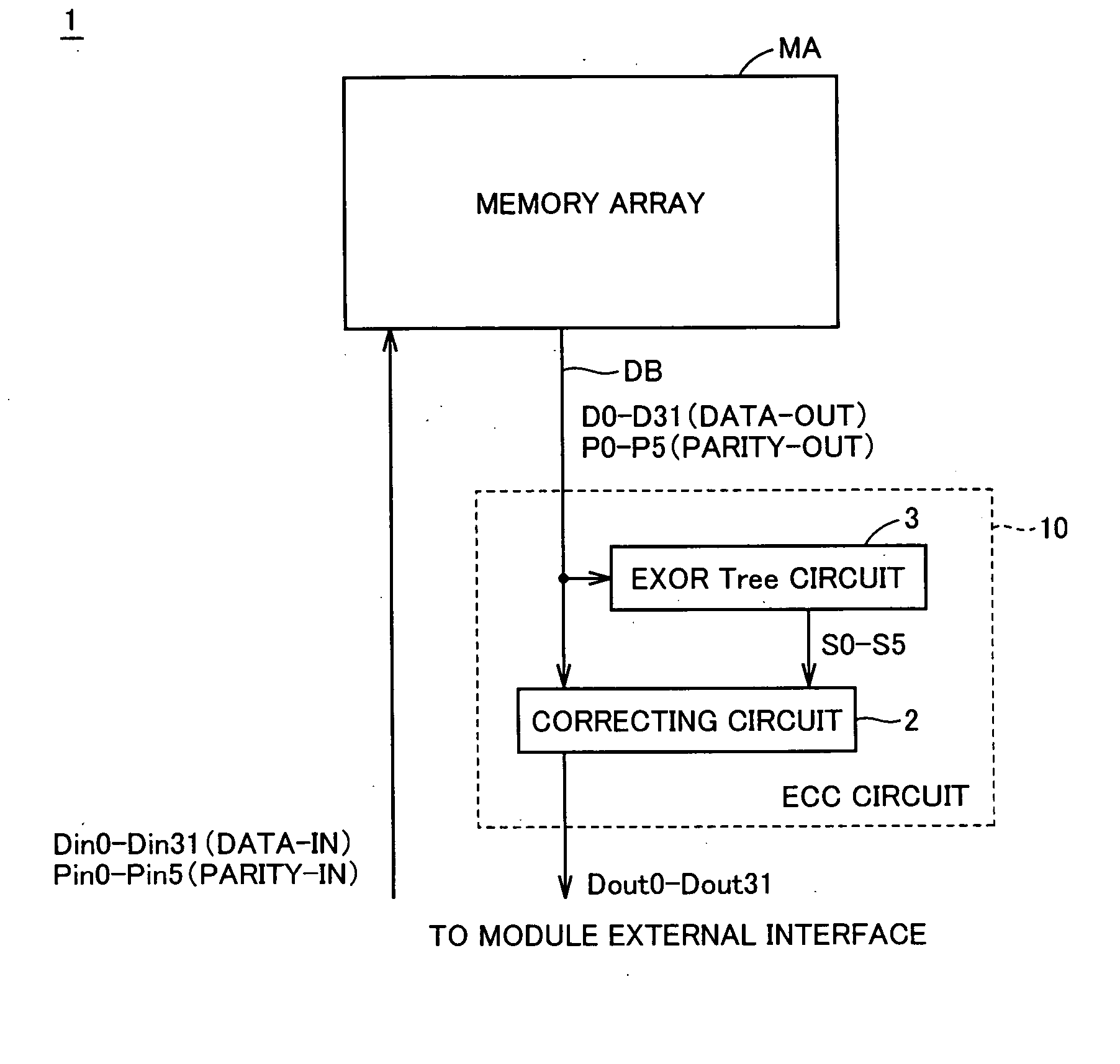
[0036] Referring to FIG. 1, a semiconductor device 1 according to a first embodiment of the present invention includes a memory array MA and an ECC circuit 10.

[0037] Memory array MA is provided to store regular data corresponding to the information amount of 32 bits. Parity bits of 6 bits are also applied and stored in memory array MA for the purpose of executing error correction on the 32 data bits.

[0038] As shown in FIG. 1, 32 information bits, i.e. data Din0-Din31, and also 6 bits of parity bits, i.e. Pin0-Pin5 to check the information bits, are applied to memory array MA (data-in, parity-in).

[0039] In a data read out operation from memory array MA, data is applied to ECC circuit 10 via a data bus DB for execution of error correction processing. Specifically, data bits D0-D31 and parity bits P0-P5 stored in memory array MA are applied to ECC circuit 10 (data-out, parity-out).

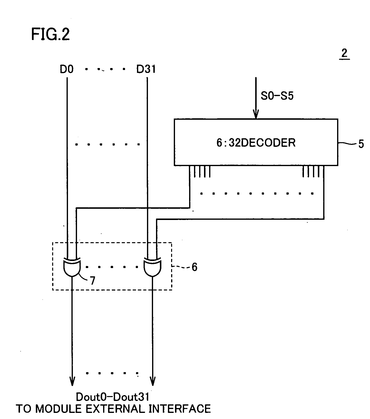
[0040] ECC circuit 10 of the first embodiment includes a correcting circuit 2 and an EXOR Tree circuit...

second embodiment

[0102] A parity check table according to a second embodiment of the present invention will be described with reference to FIGS. 11A and 11B.

[0103] The second embodiment corresponds to the case where data bits of 64 bits and 7 parity bits are stored in memory array MA.

[0104] A parity check table is set according to the scheme described with reference to FIG. 3. In the second embodiment, the values of 7 bits represented in binary numbers are allocated with respect to respective data bits and parity bits such that the values of 7 bits differ. Further, the sum of matrix elements in each row and each column of check matrix H is set so as to become lower than a predetermined value. The sum in the horizontal direction (column direction in check matrix H) is set to 4 or below. The sum in the vertical direction (row direction in check matrix H) is set to be 28 or below.

[0105] Referring to FIG. 12A, a parity circuit PC6# constituting EXOR Tree circuit 3 is formed of a plurality of XOR gate...


PUM


Abstract

In an exclusive OR circuit (XOR gate) constituting an ECC circuit, the drivability of P channel MOS transistors is set larger than the drivability of N channel MOS transistors. Accordingly, the speed of the logic level of an output node being set to an H level from an L level identified as a reset state is increased than the case where the drivability is set equal. Thus, the time required to output a syndrome from a plurality of stages of XOR gates can be reduced to allow execution of error correction processing at high speed.

Description

BACKGROUND OF THE INVENTION [0001] 1Field of the Invention [0002] The present invention relates to a semiconductor device including an error correcting circuit (ECC). [0003] 2. Description of the Background Art [0004] In semiconductor devices such as semiconductor memory devices, bit errors caused by hardware failure are encountered. There is also known a phenomenon called “soft error”, caused by the generation of pairs of electrons and holes in the silicon substrate when radiation such as α rays and neutron rays present in nature is introduced into the chip, leading to the possibility of destroying, in the worst case, data stored in the storage node of a memory cell. [0005] Reflecting the recent progress in semiconductor processing, i.e. development in microminiaturization, the size of the storage element per se has been reduced in contrast to the increase of the storage capacity. The capacity of the storage node storing data has become smaller. It is known that the resistance with...

Claims


Application Information

Patent Timeline
Patent Type & Authority Applications(United States)
IPC IPC(8): G11C29/00
CPCG06F11/1008
Inventor KAWAGOE, TOMOYAOOISHI, TSUKASA
Owner RENESAS ELECTRONICS CORP
Why Eureka
Try Eureka