I/O circuit power routing system and method

a circuit power routing and circuit technology, applied in the field of integrated circuits, can solve the problems of increasing the dynamic power dissipation of the chips, increasing the chip power dissipation, and increasing the static power, so as to increase the dynamic power, increase the static power, and increase the dynamic power

Inactive Publication Date: 2005-12-29
IBM CORP
View PDF11 Cites 18 Cited by
  • Summary
  • Abstract
  • Description
  • Claims
  • Application Information

AI Technical Summary

Benefits of technology

[0014] In one aspect, the present invention is directed to a method of floorplanning an integrated circuit chip. The method includes: a) routing a plurality of power routes corresponding to a plurality of integrated circuits using an initial width for each of the plurality of power routes; b) performing at least one electrical check of the plurality of integrated circuits; c) determining whether any one or more of the plurality of power routes has at least one electrical violation; d) for each one of said plurality of power routes having at least one electrical violation, assigning that one of the plurality of power routes a new width greater than the initial width and e) repeating steps b) and c) at least once using the one or more new widths assigned in step d) and any of the initial widths remaining after step d).
[0015] In another aspect, the present invention is directed to a system for floorplanning an integrated circuit chip that includes a plurality of integrated circuits electrically connected to one or more power distribution networks via a corresponding plurality of p...

Problems solved by technology

Higher operating frequencies result in an increase in the dynamic power dissipated by the chips.
Higher integration densities increase the number of transistors on the chip and accordingly increase the chip power dissipation.
Furthermore, leakage power, also referred to as static power, is increasing significantly from one technology to the next.
While excessive voltage drops may cause functional failures, less severe voltage drops increase gate delays, which affect chip timing and make it harder to meet a chip's timing requirements.
Higher current densities and reduced sheet resistivity raise the chip susceptibility to reliability concerns, such as electromigration (EM) and electrostatic discharge (ESD), both of which can cause physical damage and chip failure.
EM checks: Electromigration is an important reliability failure mechanism that is becoming a more serious concern in shrinking technologies.
A direct current in a metal wire running for a substantia...

Method used


Image

  • I/O circuit power routing system and method
  • I/O circuit power routing system and method
  • I/O circuit power routing system and method

Examples


example

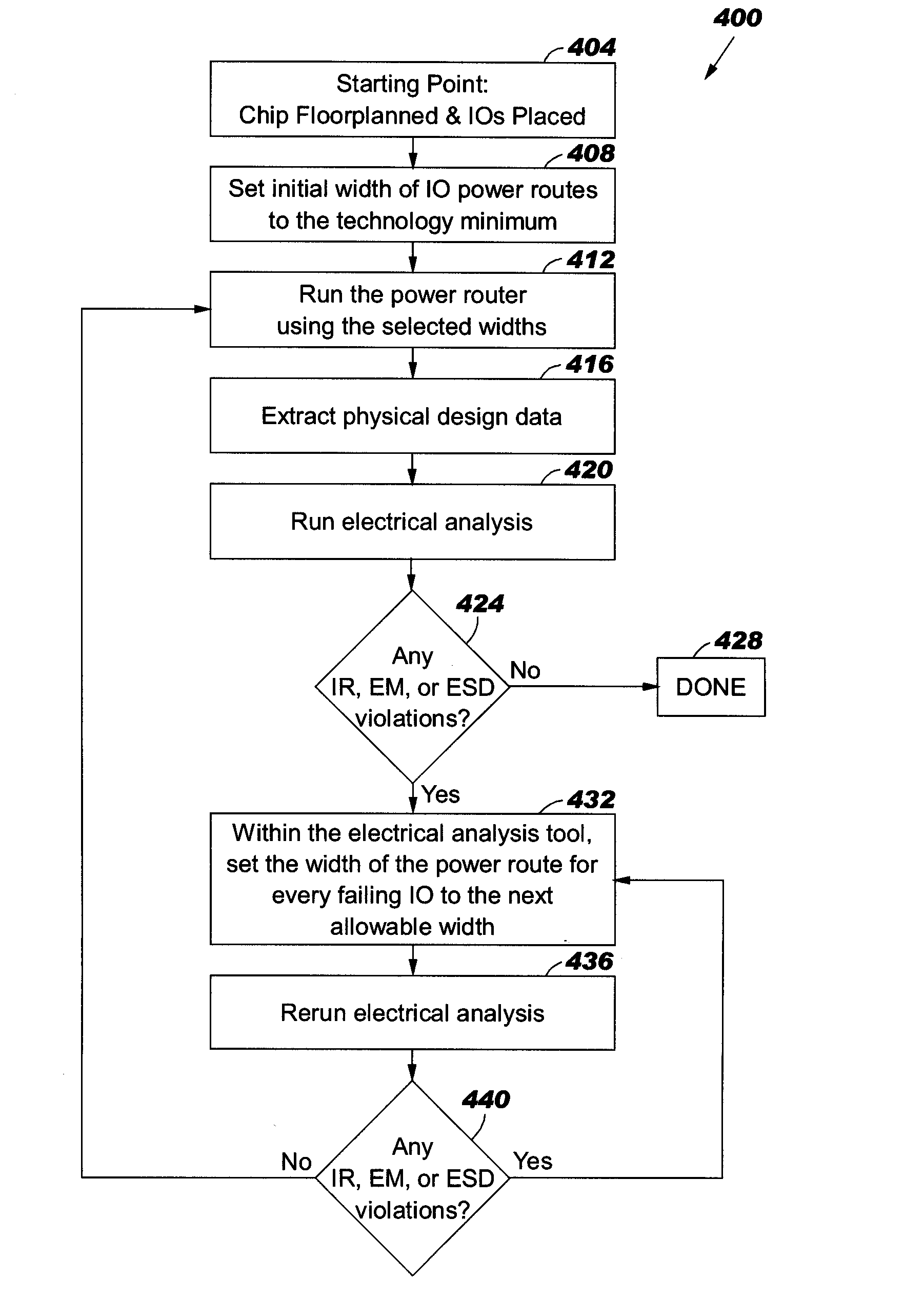
[0043] In this example, four test cases, referred to as TC1, TC2, TC3, and TC4, are considered in connection with implementing an integrated power routing method of the present invention, e.g., method 400, in connection with IR requirements. However, those skilled in the art will readily understand the modifications necessary to implement this method in connection with EM and ESD requirements as well.

[0044] The number of I / O circuits in each of test cases TC1, TC2, TC3, and TC4 is about 150 I / O circuits, as shown in Table I.

TABLE INo. of Failing I / O CircuitsNo. of I / Ovs. Power Route WidthTest CaseCircuits6 μm8 μm12 μm16 μmTC1159261030TC2152291000TC3157251041TC4145261120

[0045] The supply voltage is 1.5V for each of test cases TC1, TC2, TC3 and TC4. The other inputs for this example are the currents drawn by the various I / O circuits. For purposes of this example, it is assumed that each I / O circuit is drawing 30.0 mA of current from the power supply. In practice, the current demand...


PUM


Abstract

A method (400) of determining widths (W) and/or routes of I/O power routes (112) between one or more power distribution networks (108) and a plurality of I/O circuits (104) based on IR drop, electromigration, and electrostatic discharge electrical requirements. The method includes initially routing the I/O power routes and then iteratively analyzing the I/O power routes and iteratively incrementing the width of each power route that fails one or more of the electrical requirements until all power routes meet all electrical requirements. Once all power routes meet the electrical requirements, power routing is performed again to re-route any power routes as necessary to accommodate their wider widths. The method may be implemented in system (300) that includes a power routing tool (304), an electrical analysis tool (308), and a tool integrator (312) that implements an integrated power routing algorithm (316).

Description

BACKGROUND OF INVENTION [0001] 1. Field of the Invention [0002] The present invention generally relates to the field of integrated circuits. In particular, the present invention is directed to an I / O circuit power routing system and method. [0003] 2. Background of the Invention [0004] Thus far, the semiconductor industry has succeeded in pushing forward the famous Moore's law on technology scaling. This continuous push results in future very large scale integration (VLSI) designs characterized by higher integration densities, higher operating frequencies, and reduced feature size. Reduced feature size leads to higher sheet resistivity for the metal wires that connect electrical devices to their corresponding electrical networks. Higher operating frequencies result in an increase in the dynamic power dissipated by the chips. Higher integration densities increase the number of transistors on the chip and accordingly increase the chip power dissipation. [0005] Furthermore, leakage powe...

Claims


Application Information

Patent Timeline
IPC IPC(8): G06F9/45G06F9/455G06F17/50
CPCG06F17/5077Y02E60/76Y04S40/22G06F2217/78G06F30/394G06F2119/06Y02E60/00Y04S40/20
Inventor KOZHAYA, JOSEPH N.RYAN, PATRICK M.
Owner IBM CORP
Why Eureka
Try Eureka