Semiconductor device having CMOS driver circuit

Inactive Publication Date: 2006-01-05
RENESAS ELECTRONICS CORP
View PDF4 Cites 6 Cited by
  • Summary
  • Abstract
  • Description
  • Claims
  • Application Information

AI Technical Summary

Benefits of technology

[0030] It is an object of the present invention to provide a semiconductor device capable of suppressing the gate leak current of a

Problems solved by technology

However, as transistor microfabrication technique advances, a gate oxide film becomes thinner and a so-called gate leak current which is carried from a gate to a source or a drain or a substrate disadvantageously increases.
Recently, however, as the microfabrication technique has developed and demand for acceleration of operation rate has been rising, the thickness of a gate oxide film decreases and the gate leak current cannot be ignored.
In this way, as

Method used


Image

  • Semiconductor device having CMOS driver circuit
  • Semiconductor device having CMOS driver circuit
  • Semiconductor device having CMOS driver circuit

Examples


first embodiment

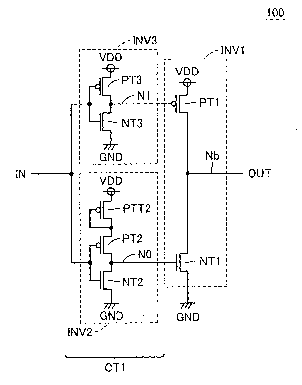
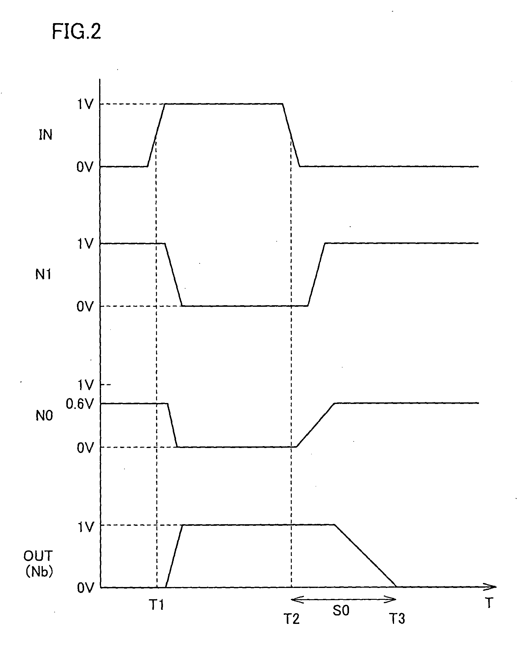
[0072] Referring to FIG. 1, a driver circuit 100 according to a first embodiment of the present invention includes inverters INV1 to INV3. Driver circuit 100 differs from a conventional driver circuit in that inverter INV0 described with reference to FIG. 18 is eliminated and two inverter stages receiving input signal IN are provided. Specifically, inverter INV2 outputs its output result to a node N0 connected to the gate of transistor NT1 of inverter INV1 in response to input signal IN. Inverter INV3 outputs its output result to node N1 connected to the gate of transistor PT1 of inverter INV1 in response to input signal IN. Inverters INV2 and INV3 constitute a control circuit CT1 which controls the voltage levels of nodes N0 and N1.

[0073] Inverter INV2 includes transistors PTT2, PT2 and NT2. It is assumed herein that transistors PTT2 and PT2 are P-channel transistors. In addition, it is assumed herein that transistor NT2 is an N-channel transistor. In transistor PTT2, a source sid...

second embodiment

[0085] Referring to FIG. 4, a driver circuit 200 according to a second embodiment of the present invention differs from driver circuit 100 shown in FIG. 1 in that a timing circuit 10 which adjusts the voltage level of an internal node for a predetermined period is further provided. Since the other constituent elements of driver circuit 200 are the same as those of driver circuit 100 in the first embodiment, they will not be described herein repeatedly. In addition, inverters INV2 and INV3 and timing circuit 10 constitute a control circuit CT2 which controls the voltage levels of nodes N0 and N1.

[0086] Timing circuit 10 includes transistors 1 and 2 and an inverter 3. It is assumed herein that transistors 1 and 2 are P-channel MOS transistors. Transistors 1 and 2 are connected in series between power supply voltage VDD and node N0 and the gate of transistor 1 receives the input of input signal IN. The gate of transistor 2 receives the input of the inverted signal of output signal OUT...

third embodiment

[0103] Referring to FIG. 8, a driver circuit 300 according to a third embodiment of the present invention differs from the driver circuit according to the second embodiment described with reference to FIG. 4 in that timing circuit 10 is replaced by a timing circuit 40. Timing circuit 40 includes a transistor 41 and an inverter 42. It is assumed herein that transistor 41 is a P-channel MOS transistor as one example. Transistor 41 is arranged between nodes N1 and N0 and the gate thereof receives the input of the inverted signal of output signal OUT through inverter 42. In addition, inverters INV2 and INV3 and timing circuit 40 constitute a control circuit CT3 which controls the voltage levels of nodes N0 and N1.

[0104] Timing circuit 40, similarly to timing circuit 20, temporarily, electrically couples power supply voltage VDD to node N0 when transistor NT1 is turned on. Specifically, if output signal OUT is 1 V (“H” level), transistor 41 is turned on and nodes N1 and N0 are electrica...


PUM


Abstract

Voltages of nodes are controlled in accordance with an input signal using inverters. A voltage level of a transistor is adjusted using a transistor included in the inverter. By setting a gate voltage supplied to a gate of the transistor lower than a power supply voltage and higher than an ON-state voltage, gate leakage current of the transistor can be greatly decreased.

Description

BACKGROUND OF THE INVENTION [0001] 1. Field of the Invention [0002] The present invention particularly relates to a semiconductor device having a CMOS driver circuit. [0003] 2. Description of the Background Art [0004] In recent years, semiconductor devices each including a plurality of processing circuits have been produced as one-chip microcomputers and these semiconductor devices have been utilized for electronic circuit equipment or the like of, for example, cellular phones. While a portable equipment such as a cellular phone necessarily employs a battery as a power supply, the battery is made small in size and light in weight to satisfy the demand to do so. [0005] Since it is demanded to employ the battery for long time besides such a demand for making the battery small in size and light in weight, it is strongly demanded to decrease the power consumption of the battery. On the other hand, for a digital cellular phone or the like, it is further demanded to accelerate the semicon...

Claims


Application Information

Patent Timeline
IPC IPC(8): H03B1/00H01L21/822H01L27/04H03K17/16H03K17/687H03K19/00H03K19/0175H03K19/0948
CPCH03K19/0013H03K19/00
Inventor NII, KOJI
Owner RENESAS ELECTRONICS CORP
Why Eureka
Try Eureka