Semiconductor device including a trench-type metal-insulator-metal (MIM) capacitor and method of fabricating the same

a metal-insulator-metal and capacitor technology, applied in semiconductor devices, capacitors, electrical devices, etc., can solve the problems of increasing the capacitance deviation between capacitors and the leakage current, and achieve the effect of stably providing the desired capacitance, preventing the damage of the dielectric layer, and improving process stability

Inactive Publication Date: 2006-01-12
SAMSUNG ELECTRONICS CO LTD
View PDF7 Cites 29 Cited by
  • Summary
  • Abstract
  • Description
  • Claims
  • Application Information

AI Technical Summary

Benefits of technology

[0032] According to an embodiment of the present invention, a stress on a trench edge portion, which is structurally vulnerable during the fabrication of the trench-type MIM capacitor, may be reduced, and a generation of leakage current and device defects due to the d

Problems solved by technology

As a result, the dielectric layer 24 may be damaged, thereby increasing a leakage current a

Method used


Image

  • Semiconductor device including a trench-type metal-insulator-metal (MIM) capacitor and method of fabricating the same
  • Semiconductor device including a trench-type metal-insulator-metal (MIM) capacitor and method of fabricating the same
  • Semiconductor device including a trench-type metal-insulator-metal (MIM) capacitor and method of fabricating the same

Examples


Embodiment Construction

[0036] Korean Patent Application No. 2004-52971, filed on Jul. 8, 2004, in the Korean Intellectual Property Office, and entitled: “Semiconductor Device Having Trench-type Metal-Insulator-Metal Capacitor and Method of Fabricating the Same,” is incorporated by reference herein in its entirety.

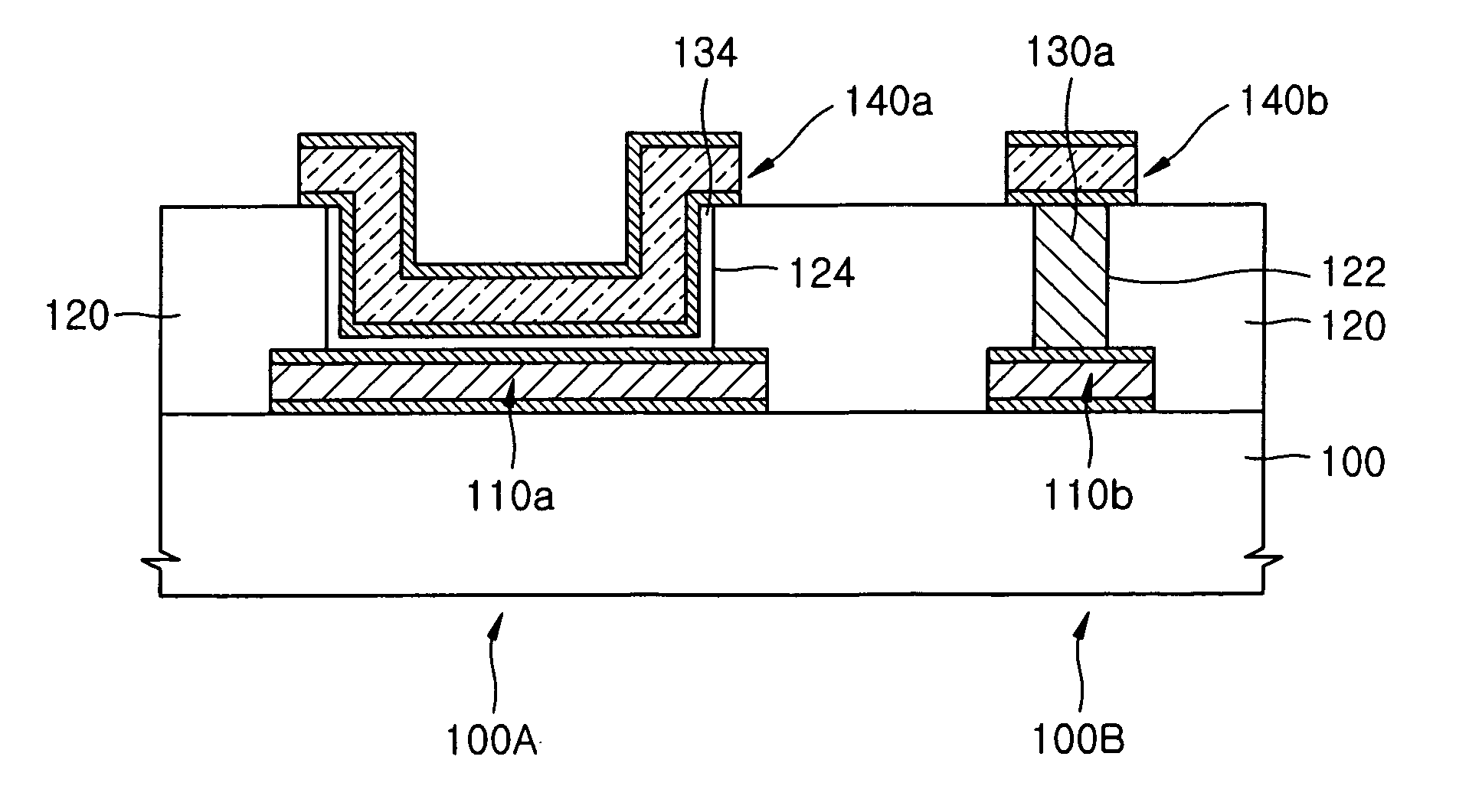
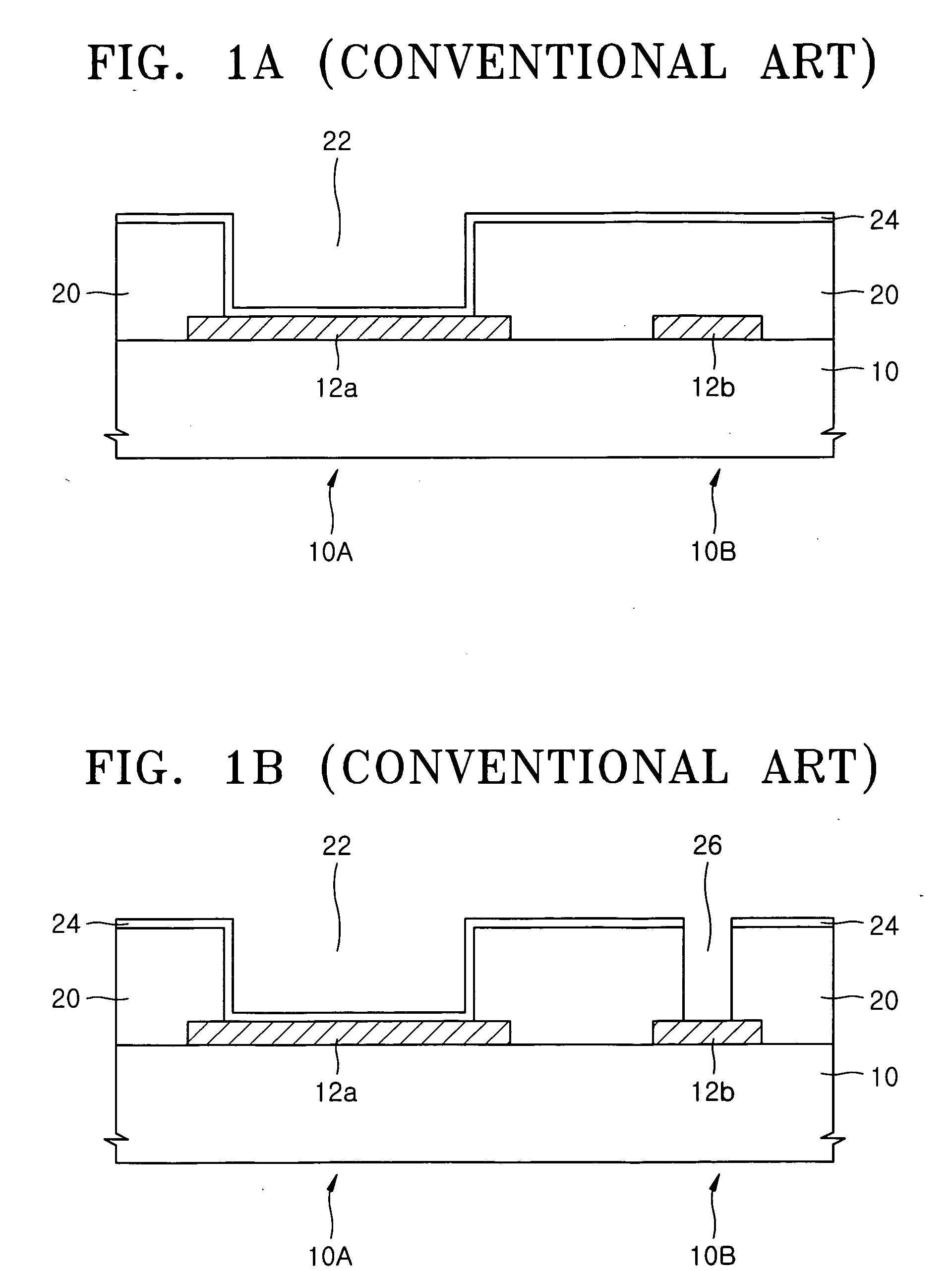
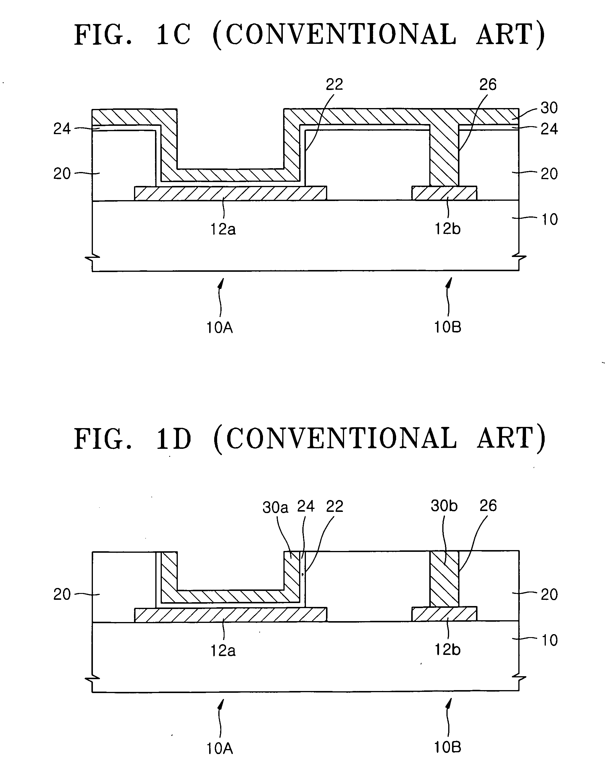
[0037] The present invention will now be described more fully hereinafter with reference to the accompanying drawings, in which exemplary embodiments of the invention are shown. The invention may, however, be embodied in different forms and should not be construed as limited to the embodiments set forth herein. Rather, these embodiments are provided so that this disclosure will be thorough and complete, and will fully convey the scope of the invention to those skilled in the art. In the figures, the dimensions of films, layers and regions are exaggerated for clarity of illustration. It will also be understood that when a layer is referred to as being “on” another layer or substrate, it can be di...


PUM


Abstract

In a semiconductor device, and a method of fabricating the same, the semiconductor device includes a bottom electrode and a first interconnection layer on a semiconductor substrate, an upper surface of the bottom electrode and an upper surface of the first interconnection layer being level, an interlayer insulating layer having a trench exposing the upper surface of the bottom electrode and a via hole exposing the upper surface of the first interconnection layer, a contact plug formed of a first material inside the via hole and connected to the first interconnection layer, an upper electrode formed of a second material inside the trench on the bottom electrode, the first material being exclusive of the second material, and a dielectric layer interposed between the bottom electrode and the upper electrode, and formed only inside the trench.

Description

BACKGROUND OF THE INVENTION [0001] 1. Field of the Invention [0002] The present invention relates to a semiconductor device and a method of fabricating the same. More particularly, the present invention relates to a semiconductor device including a trench-type metal-insulator-metal (MIM) capacitor and a method of fabricating the same. [0003] 2. Description of the Related Art [0004] A capacitor as a passive component is used for various purposes in order to provide various logic circuits. Recently, demand for a capacitor having high capacitance has greatly increased. In particular, in the fabrication of a semiconductor device by employing analog circuits in a merged DRAM with logic (MDL), in which a DRAM and a logic circuit are merged, a metal-insulator-metal (MIM) capacitor as a capacitor of an analog circuit or a logic circuit is formed to provide the capacitance characteristics of the analog circuit. [0005]FIGS. 1A through 1F illustrate cross-sectional views of processing sequence...

Claims


Application Information

Patent Timeline
IPC IPC(8): H01L27/108H01L21/8242
CPCH01L28/75H10B12/00
Inventor PARK, DUK-SEOPARK, HYUNG-MOO
Owner SAMSUNG ELECTRONICS CO LTD
Why Eureka
Try Eureka