Semiconductor integrated circuit design method, design support system for the same, and delay library

a technology of integrated circuits and support systems, applied in the direction of error detection/correction, program control, instruments, etc., can solve the problem of extreme difficulty in controlling lens aberration, and achieve the effect of precise design margin and easy creation of present invention

Inactive Publication Date: 2006-01-12
PANASONIC CORP
View PDF1 Cites 16 Cited by
  • Summary
  • Abstract
  • Description
  • Claims
  • Application Information

AI Technical Summary

Benefits of technology

[0026] In the delay library of the present invention, the delay values of the cells are stored on a per cell layout direction basis and on a per exposure apparatus basis which is used for exposure. Accordingly, delay simulation to a logic circuit using the delay library of the present invention enables timing verification according to each layout direction of the cells layouted on a waver. Hence, no influence of cell layout direction is involved, enabling precise margin of the design.
[0027] In the delay library according to the present invention, it is preferable that one of the plurality of cells is set as a representative cell, first delay values in each of a plurality of layout directions in each of a plurality of exposure apparatuses of the representative cell are calc

Problems solved by technology

A method of controlling the lens aberration can be considered as a method for solving the problem of the phenomenon that the device characteristic depends on the cell layout direction through a p

Method used


Image

  • Semiconductor integrated circuit design method, design support system for the same, and delay library
  • Semiconductor integrated circuit design method, design support system for the same, and delay library
  • Semiconductor integrated circuit design method, design support system for the same, and delay library

Examples


first embodiment

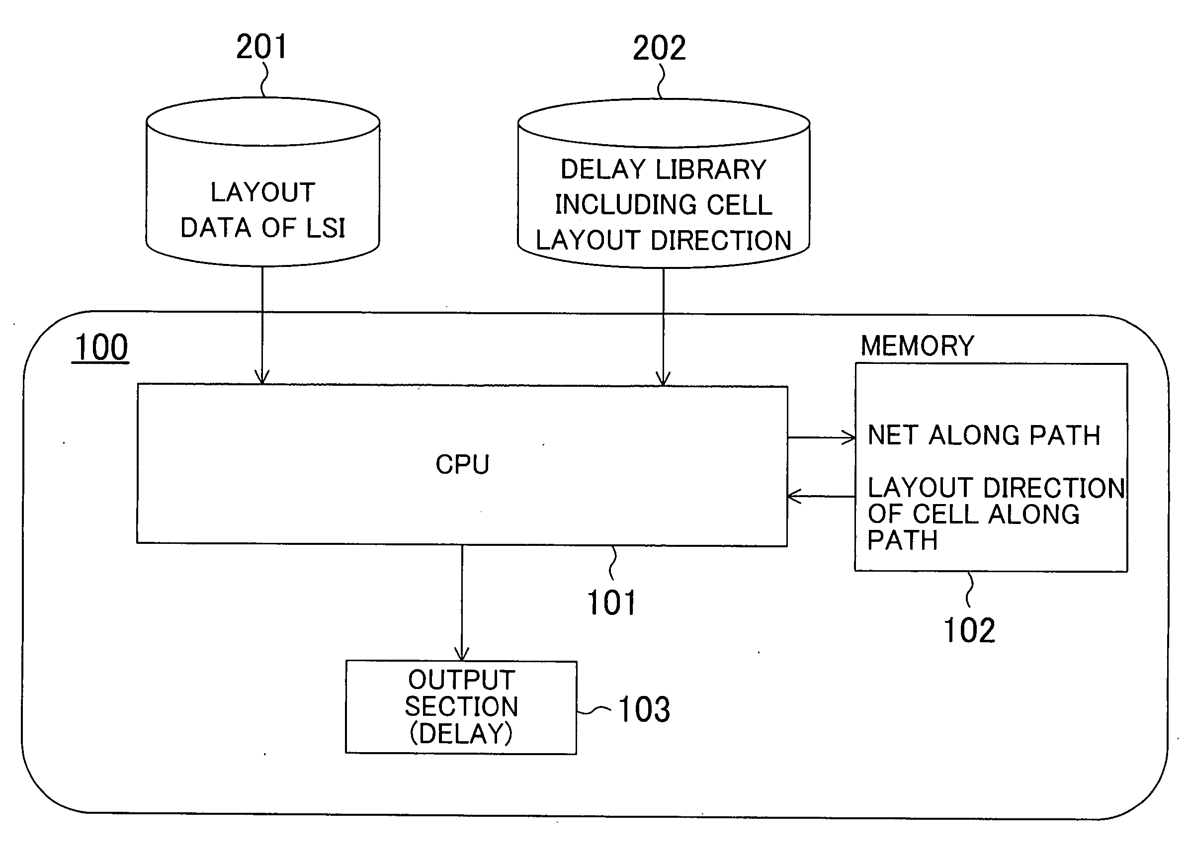
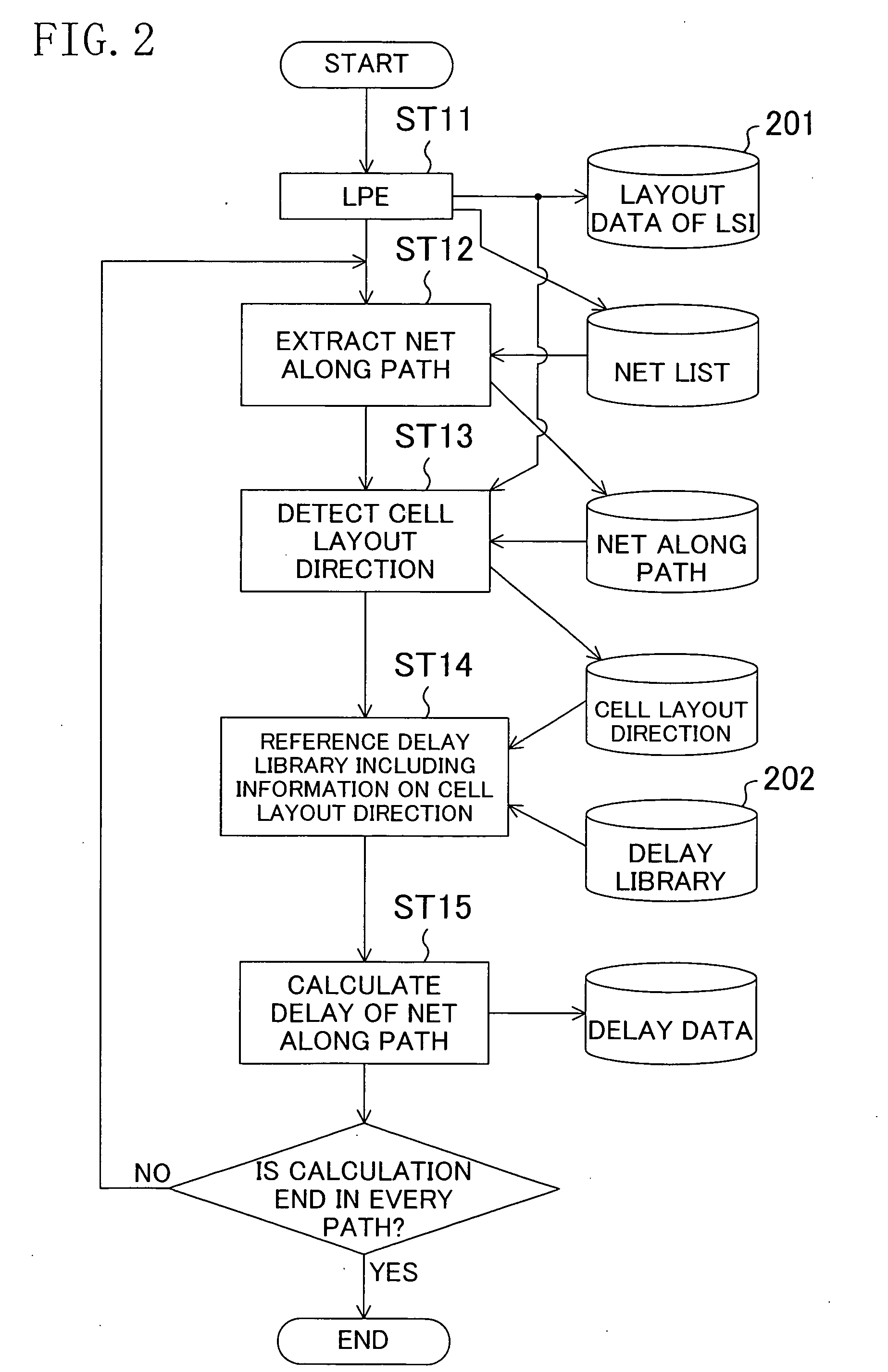
[0040] A first embodiment of the present invention will be descried with reference to the drawings. FIG. 1 shows a constitution in blocks of a semiconductor integrated circuit design support system according to the first embodiment of the present invention, and FIG. 2 shows a semiconductor integrated circuit design method using the design support system and depicts a flow for timing verification of a large scale semiconductor integrated circuit (LSI).

[0041] As shown in FIG. 1, the design support system 100 is a workstation, for example and is composed of a CPU 101, a main memory 102, and output section 103.

[0042] In delay calculation, layout data 201 of an LSI to be verified and a delay library 202 including each layout direction of cells of a cell group composing the LSI to be verified are read.

[0043] Operation of the semiconductor integrated circuit design support system constituted as above will be described below with reference to FIG. 2.

[0044] As shown in FIG. 2, the layout...

second embodiment

[0059] A second embodiment of the present invention will be described below with reference to the drawings.

[0060] In the second embodiment, a method for creating a delay library having delay data of each cell layout direction and of each lot of exposure apparatuses will be described.

[0061]FIG. 5 depicts a processing flow of a delay library creation method that introduces delay variation dependent on the exposure apparatus lots and on the cell layout directions according to the second embodiment of the present invention. In detail, FIG. 5 shows a sequence for calculating a delay in cell level between a gate length of a MOS transistor at a design stage in the layout data 201 including a cell as a minimum layout unit of an LSI to be simulated and a gate length subjected to the semiconductor device process.

[0062] As shown in FIG. 5, a lot of an exposure apparatus to be used for exposure and a cell layout angle are first selected by referencing the layout data 201 of the LSI in a step...

third embodiment

[0070] A third embodiment of the present invention will be described below with reference to the drawings.

[0071] In the third embodiment, another method for creating a delay library having delay data of each cell layout direction and of each exposure apparatus lot will be described.

[0072] In the second embodiment, the delay library 202 is created from the net list created by optical simulation and LPE to all cell data of the layout data 201 of the LSI. While in the third embodiment, a representative cell is selected from the layout data 201, each delay characteristic variation coefficient of each exposure apparatus lot and of each cell layout angle in the selected representative cell is obtained, and then, the delay characteristic variation coefficients are multiplied to the other cells, thereby obtaining delay values dependent on every exposure apparatus lot and on every cell layout angle.

[0073]FIG. 7 is a flowchart depicting a method for creating a delay library introducing var...


PUM


Abstract

In a semiconductor integrated circuit design method for simulating a delay of a logic circuit based on delay values which are calculated for each kind of a plurality of cells composing the logic circuit or for each signal path of the logic circuit and which are stored in a delay library, the simulation is performed to a block including at least one cell, and a delay value varying dependent on a layout direction of the cell included in the block is used as the delay value in the delay library. By this method, timing verification can be performed according to the layout direction of each cell layouted on a wafer, attaining precise margin of the design and improving yield of the semiconductor integrated circuit.

Description

CROSS REFERENCE TO RELATED APPLICATIONS [0001] This Non-provisional application claims priority under 35 U.S.C. § 119(a) on Patent Application No. 2004-200058 filed in Japan on Jul. 7, 2004, the entire contents of which are hereby incorporated by reference. BACKGROUND ART [0002] The present invention relates to a semiconductor integrated circuit design method for calculating by simulating a delay of a signal that propagates in a logic circuit in designing a large scale integrated circuit (LSI) including a MIS transistor, a design support system therefor, and a delay library. [0003] Recently, miniaturization of patterns (circuit patterns) in semiconductor devices are being promoted at a feverish pace for increasing integration and enhancing performance of LSIs including MOS transistors. In association with the pattern miniaturization, patterns are formed at around the critical level of a logical resolution in a lithography step, and therefore, optical proximity effect and lens aberra...

Claims


Application Information

Patent Timeline
IPC IPC(8): G06F17/50
CPCG06F17/5031G06F30/3312
Inventor TAMAKI, YASUHIROYAMASHITA, KYOJI
Owner PANASONIC CORP
Why Eureka
Try Eureka