Differential clock input buffer

a differential clock and input buffer technology, applied in the field of digital clock input buffers, can solve the problems of adding noise to the resulting output, and the single latch stage provided by the second stage will still exhibit some level of jitter, so as to improve the hysteresis of input, improve the noise immunity, and improve the effect of duty cycle control

Inactive Publication Date: 2006-01-19
KENET
View PDF10 Cites 11 Cited by
  • Summary
  • Abstract
  • Description
  • Claims
  • Application Information

AI Technical Summary

Benefits of technology

[0013] A second stage latching circuit, which may use circuits adapted to mirror currents in the first stage, is also provided as a pair of cross coupled transistors with resistive loads. The second stage latch provides further gain, limiting, hysteresis, and latching, and is preferably biased at the center of an output buffer's range, to provide better duty cycle control over a wider range of signal levels.
[0014] The circuit provides improved input hysteresis for greater noise immunity, and limits jitter production by ensuring that the edges of the resulting clock signals are as fast as possible, while minimizing the time that the clock buffer spends in the linear region.

Problems solved by technology

For one, the use of a simple linear differential amplifier as a first stage, although designed as a low noise amplifier, will actually add noise to the resulting output.
In addition, the single latch stage provided by the second stage will still exhibit some level of jitter.

Method used


Image

  • Differential clock input buffer
  • Differential clock input buffer
  • Differential clock input buffer

Examples


Embodiment Construction

[0022] A description of preferred embodiments of the invention follows.

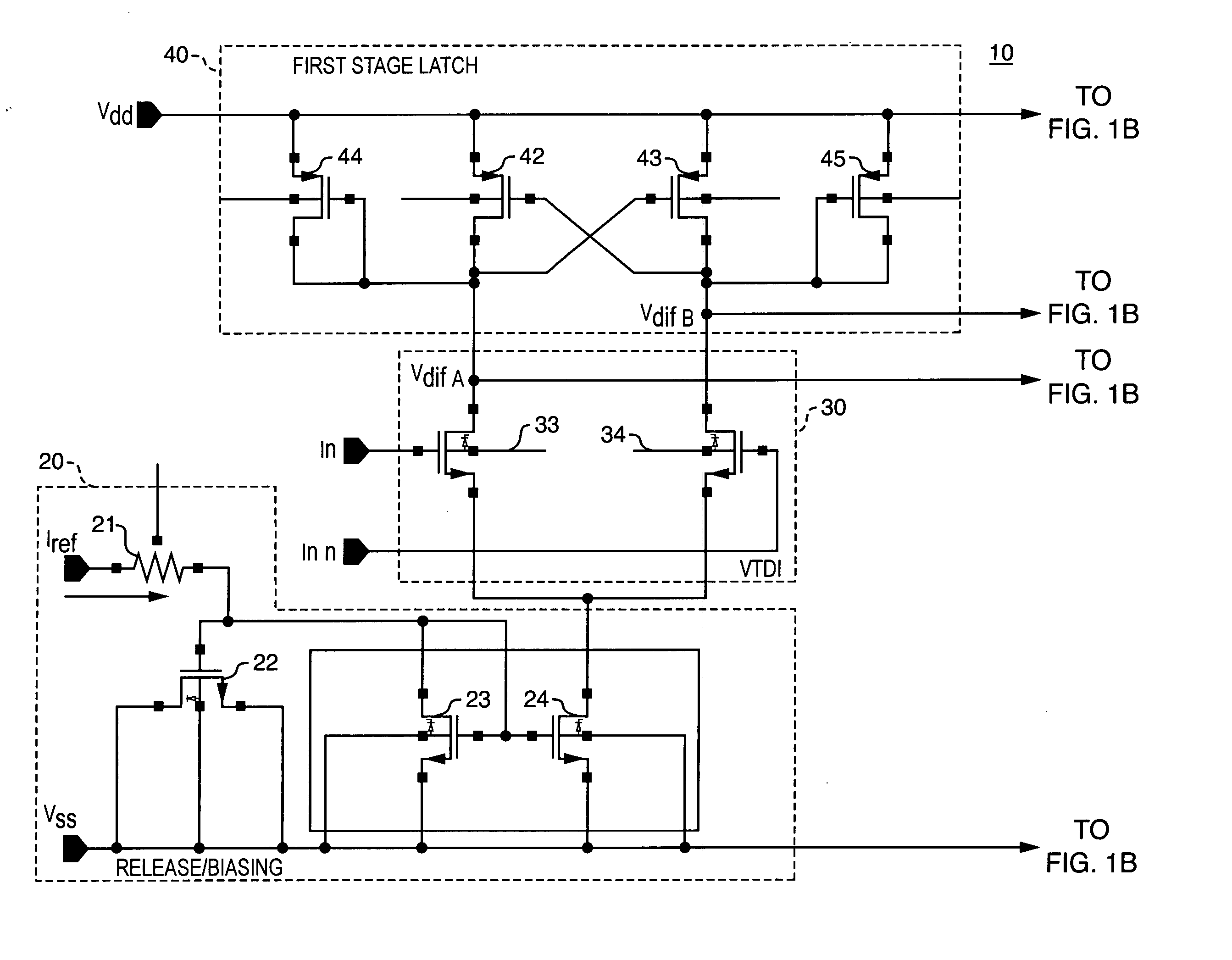
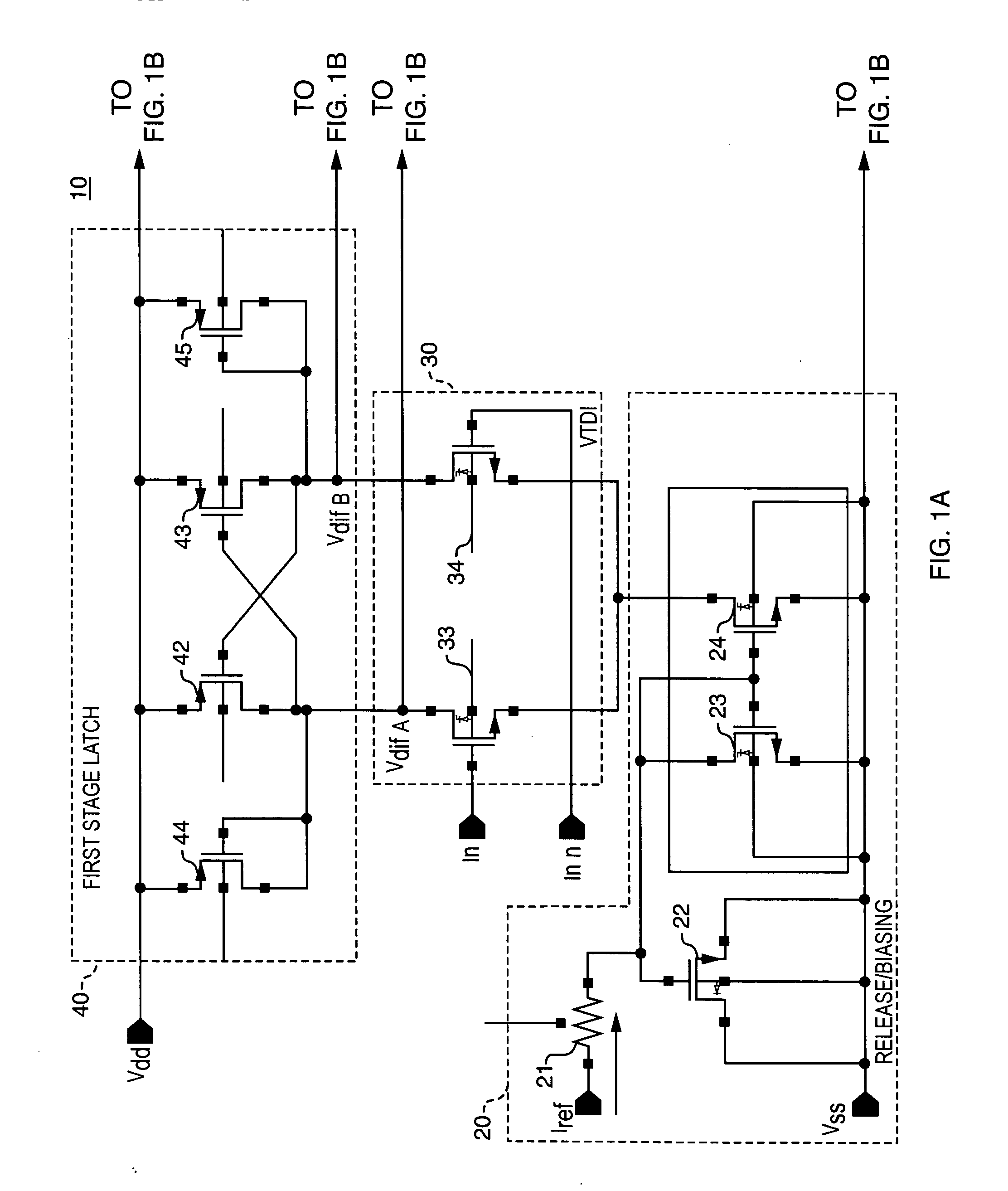
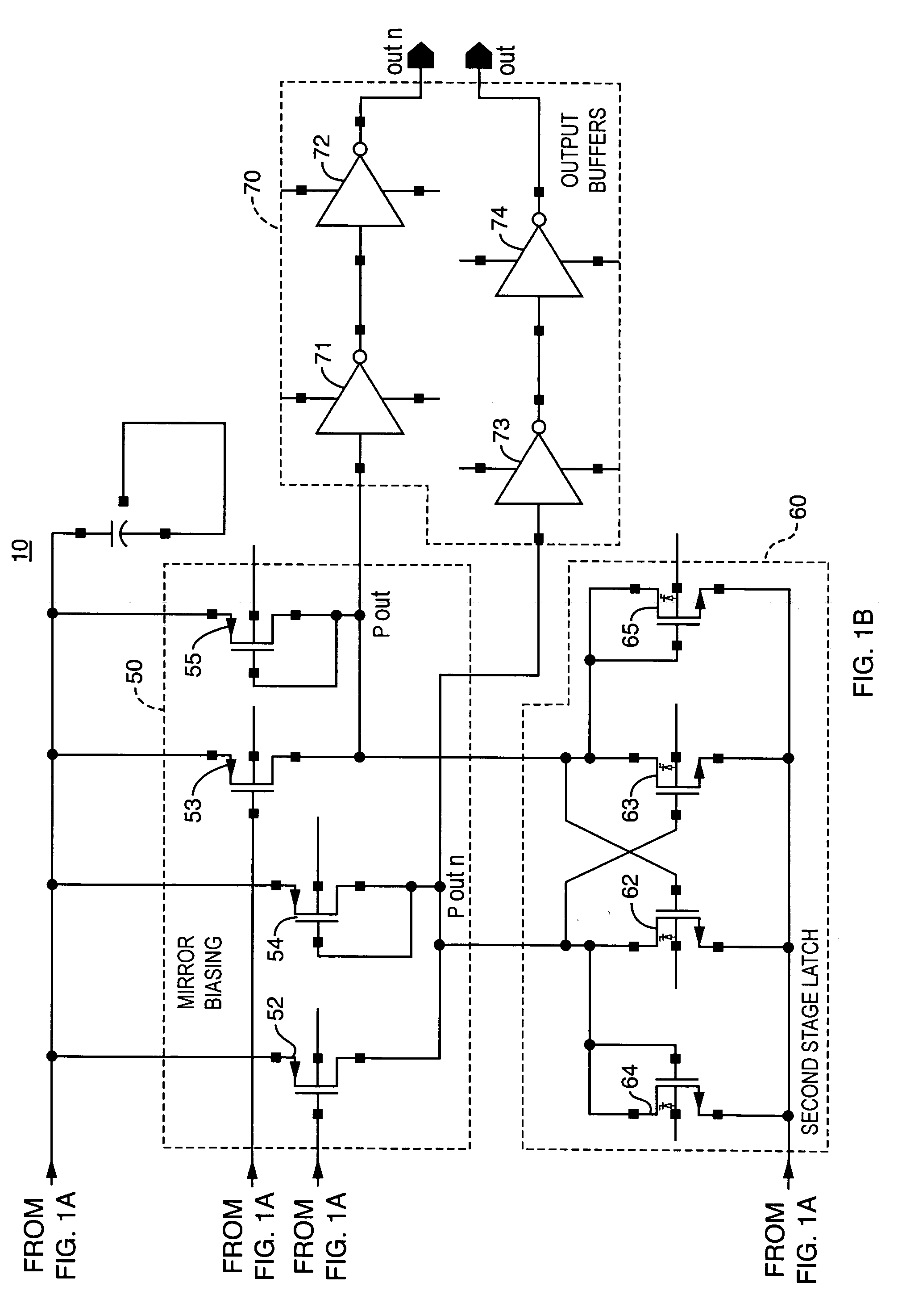
[0023]FIG. 1 is a schematic diagram of one preferred embodiment of a clock buffer circuit 10 according to the present invention. The circuit 10 consists of several functions, including a reference / biasing circuit 20, a voltage to current (V-to-I) converter (differential pair) 30, a first stage latch 40, a mirror / biasing circuit 50, a second stage latch 60, and output buffers 70.

[0024] The input signal(s) may be single or double ended. If a single ended signal, it is provided at terminal IN (or just at INN, with the other input terminal biased somewhere near vdd / 2); if double ended, they are provided to inputs IN and INN. The voltage to current converter 30 converts these input voltage(s) to differential currents at nodes VdiffA and VdiffB. The voltage to current converter 30 consists of a pair of CMOS transistors 33, 34 arranged as a differential amplifier, to provide current from a source Vss (and to reject co...


PUM


Abstract

A compact, differential clock input buffer that converts single-end or differential sine wave or square wave inputs into complementary squarewave digital outputs, with low-jitter, and 50% duty cycle outputs. Low-noise oscillator design concepts are applied to provide at least two stages of regeneration. This minimizes the time the clock buffer spends in the noise-susceptible linear region. A first stage latching circuit consists of a pair of cross coupled transistors (i.e., a differential transistor pair) with resistive loads to provide gain, limiting, hysteresis, and latching functions. These transistors operate in a linear region for only a very small range of input voltage. A second stage latching circuit, which can use a current mirror, is also provided as a pair of cross coupled transistors with resistive loads. The second stage latch provides positive feedback to further limit the linear operating range.

Description

RELATED APPLICATION(S) [0001] This application claims the benefit of U.S. Provisional Application No. 60 / 585,682, filed on Jul. 6, 2004. The entire teachings of the above application(s) are incorporated herein by reference.BACKGROUND OF THE INVENTION [0002] The present invention relates to circuits for generating digital clock signals. Many different circuits require a generation of a digital clock signal having a nearly 50% duty cycle with sharp rise and fall times. Such clock signals are typically generated using a crystal oscillator and level shifting buffer circuits that convert the crystal oscillator output to a signal having the voltage and current levels expected by logic circuits. [0003] Once such circuit is described in a paper by Riley, et al. entitled “Techniques for In-Band Phase Noise Reduction in ΔΣSynthesizers”, IEEE Transactions on Circuits and Systems—II, Analog and Digital Signal Processing, Vol. 50, No. 11, November 2003, at pages 800-802. In that circuit, a self-...

Claims


Application Information

Patent Timeline
Patent Type & Authority Applications(United States)
IPC IPC(8): H03B1/00
CPCH03K3/356113H03K5/1565H03K3/35613
Inventor KUSHNER, LAWRENCE J.
Owner KENET
Why Eureka
Try Eureka