

Charged particle beam apparatus
a particle beam and apparatus technology, applied in the field of chargeable particle beam apparatus, can solve the problems of uneven or dispersed adjustment values, more time consumed, and many time required for introducing a function, so as to reduce the time consumed to find out a function during the new design of the apparatus, and eliminate the time/technical restrictions imposed on operation per se.
- Summary
- Abstract
- Description
- Claims
- Application Information
AI Technical Summary
Benefits of technology
Problems solved by technology
Method used
Image

Examples
Embodiment Construction
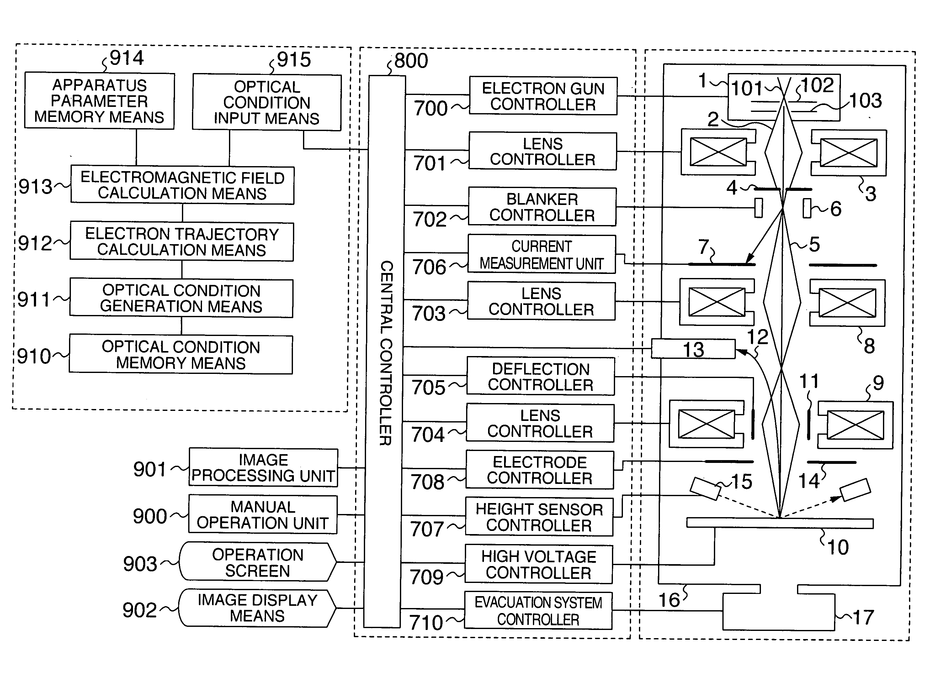
[0026] An embodiment of the present invention will now be described specifically by way of example of a semiconductor circuit pattern defect inspection apparatus based on a scanning electron microscope (hereinafter referred to as SEM type wafer inspection apparatus).
[0027] Referring to FIG. 1, construction of the SEM type wafer inspection apparatus will be described.
[0028] In an electron gun 1 controlled by an electron gun controller 700, an extracting voltage V1 applied across electron source 101 and extracting electrode 102 and thermal energy applied to the electron source 101 cooperate to emit an electron beam 2 representing a charged particle beam.
[0029] The electron beam 2 is accelerated to an outgoing energy level EO=e|Vo| by an accelerating voltage Vo applied to an accelerating electrode 103 so as to be emitted from the electron gun 1. The emitted electron beam 2 is condensed by a first condenser lens 3 controlled by a lens controller 701 and is then admitted through a bea...
PUM
 Abstract
Description
Claims
Application Information