Nitride semiconductor light emitting device

Active Publication Date: 2006-01-26
NICHIA CORP
View PDF12 Cites 50 Cited by
  • Summary
  • Abstract
  • Description
  • Claims
  • Application Information

AI Technical Summary

Benefits of technology

[0009] An object of the present invention is to provide a nitride semiconductor light emitting device, comprising a light transmitting electrode and a p-side pad electrode formed on a p-side nitride semiconductor layer so as to emit light through the light transmitting electrode, that has a novel device structure enabling it to extract light efficiently.
[0010] In the nitride semiconductor light emitting device that comprises the light transmitting electrode and the p-side pad electrode formed on the p-side nitride semiconductor layer so as to emit light through the light transmitting electrode, distribution of light in the light emerging surface is determined by such factors as the arrangement of the p-side pad electrode and the n-side pad electrode that supply the current and the shapes o

Problems solved by technology

As the nitride semiconductor light emitting device becomes smaller in size, the p-side pad electrode and the n-side pad electrode occupy a larger proportion of the surface area of the chip, thus giving rise to the problem of maintaining external quantum

Method used


Image

  • Nitride semiconductor light emitting device
  • Nitride semiconductor light emitting device
  • Nitride semiconductor light emitting device

Examples


embodiment 1

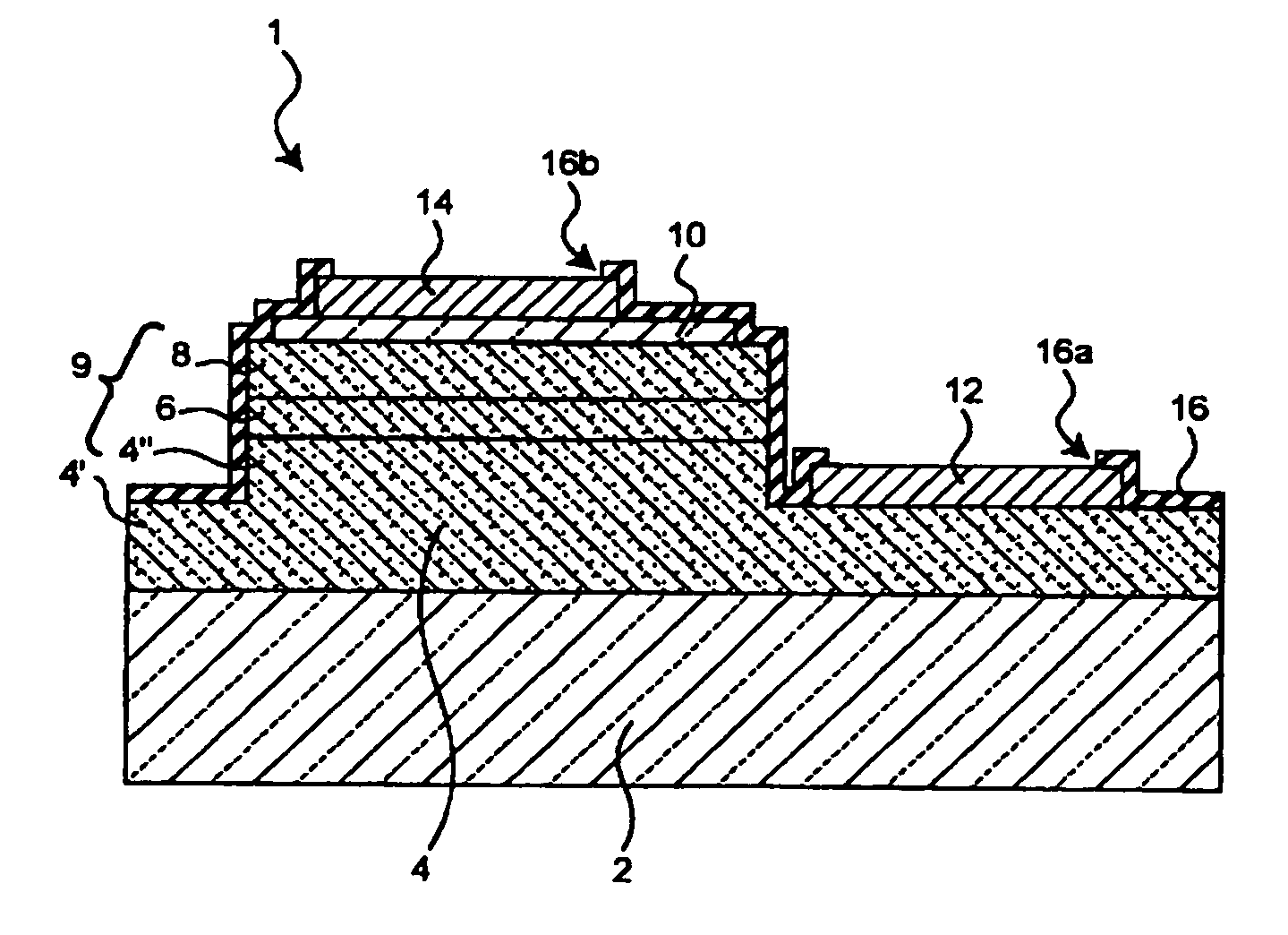
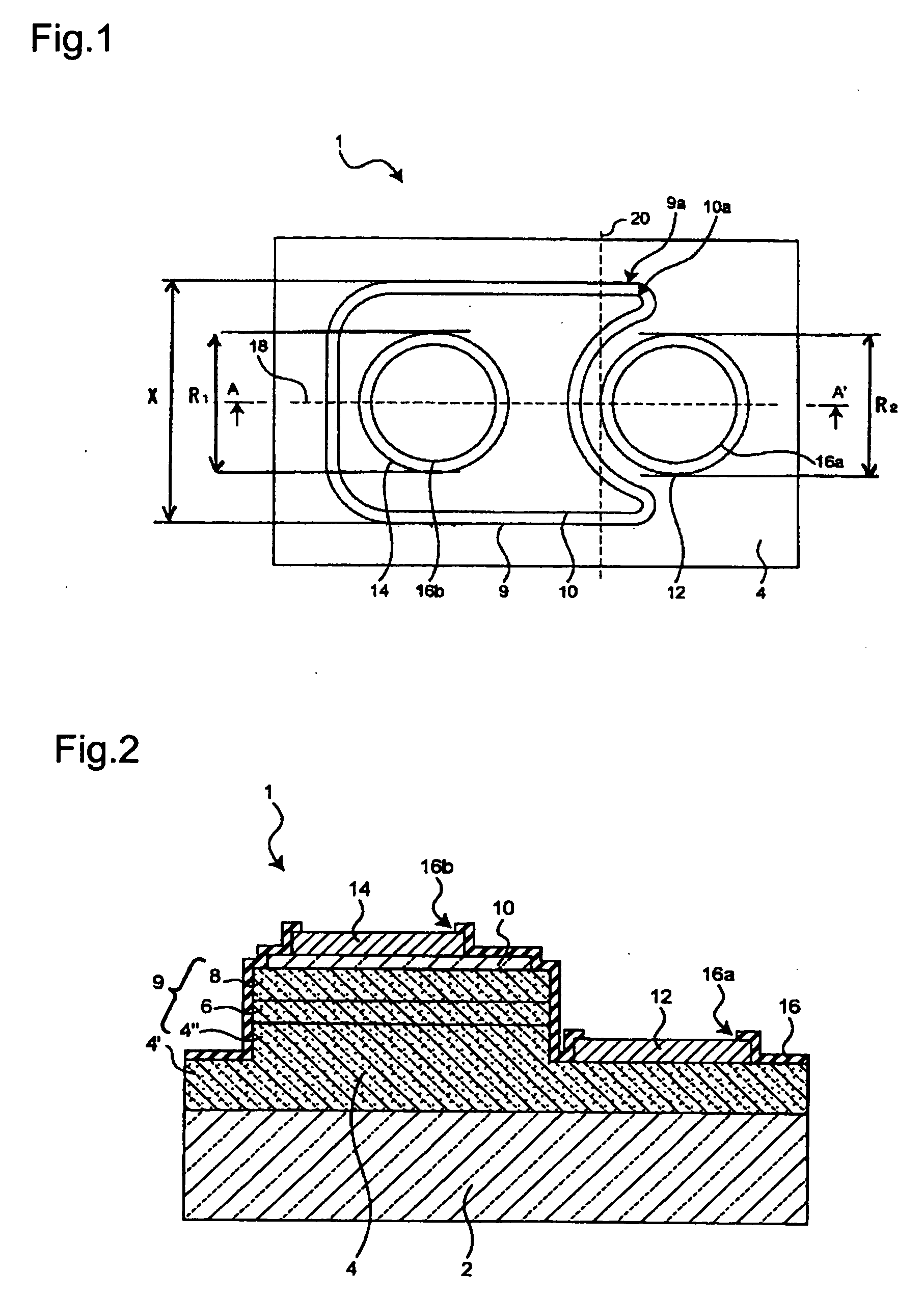
[0055]FIG. 1 is a top view of a nitride semiconductor light emitting device according to the first embodiment of the present invention, and FIG. 2 is a sectional view thereof. As shown in FIG. 2, the nitride semiconductor light emitting device 1 comprises an n-side nitride semiconductor layer 4, an active layer 6 and a p-side nitride semiconductor layer 8 formed successively on a substrate 2 made of sapphire, SiC, Si, GaN or the like, and has double hetero-junction structure. A light transmitting electrode 10 is formed from ITO or thin metal film over substantially the entire surface of the p-side nitride semiconductor layer 8, and a p-side pad electrode 14 is formed on the light transmitting electrode 10 for the connection with an external circuit by wire bonding or the like.

[0056] On the other hand, to form an n-side pad electrode 12, top portions 4″ of the p-side nitride semiconductor layer 8, the active layer 6 and the n-side nitride semiconductor layer are removed so as to exp...

embodiment 2

[0100] This embodiment is similar to Embodiment 1 except that the substrate 2 is separated by laser scribing.

[0101] Laser scribing is a method of forming separation grooves by means of laser beam. After forming the separation grooves by means of laser beam, the substrate can be separated into individual chips. Laser scribing is capable of forming a deeper and narrower groove than other methods such as dicing. This enables it to decrease the proportion of the substrate surface area occupied by the grooves so as to increase the number of chips that can be produced from one substrate. In addition, the deeper separation groove decreases the possibility of breaking failure. Thus laser scribing is suited for separating small chips.

[0102] In this embodiment, laser scribing is employed for separating the nitride semiconductor light emitting device described in Embodiment 1. This not only increases the number of chips that can be produced from one substrate and improves the yield of produc...

embodiment 3

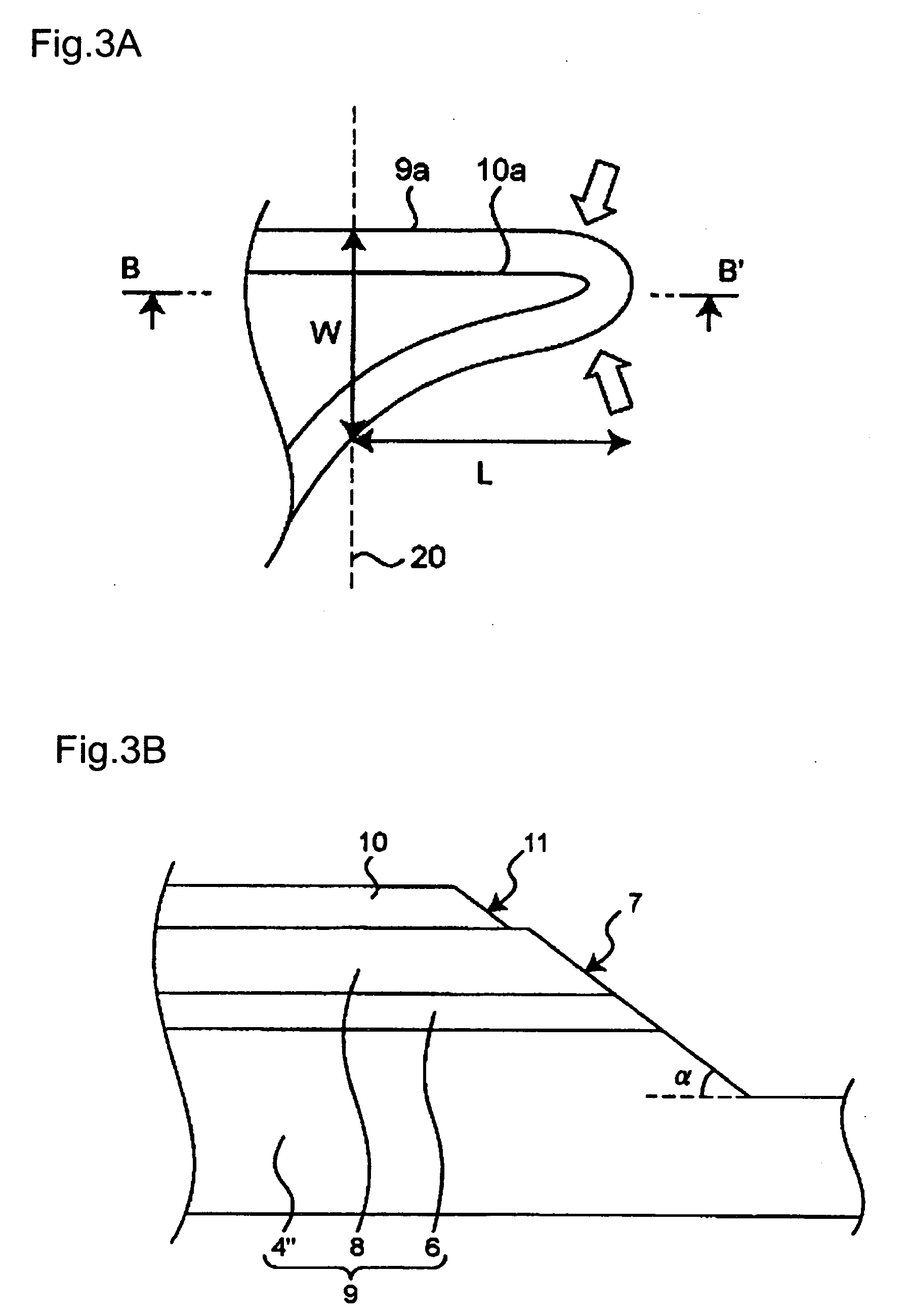
[0113]FIG. 10 is a top view showing a nitride semiconductor light emitting device according to Embodiment 2 of the present invention. This embodiment is similar to Embodiment 1 except for those described below.

[0114] In this embodiment, the n-side pad electrode 12 is formed at a position near a corner of the chip, while the p-side layer 9 extends along one side face of the n-side pad electrode 12. Assuming the centerline 18 that connects the center of the p-side pad electrode 14 and the center of the n-side pad electrode 12 and the tangent line 20 of the n-side pad electrode 12 that crosses the centerline 18 at right angles, then the extension of the p-side layer 9 is located on the side of the tangent line 20 opposite to the n-side pad electrode 14. As a result, intensity of light emission in the extension of the p-side layer 9 tends to become lower, and the decrease in intensity of light emission is more conspicuous in the distal end portion 22. In this embodiment, therefore, the...


PUM


Abstract

A nitride semiconductor light emitting device comprising an n-side nitride semiconductor layer and a p-side nitride semiconductor layer formed on a substrate, with a light transmitting electrode 10 formed on the p-side nitride semiconductor layer, and the p-side pad electrode 14 formed for the connection with an outside circuit, and the n-side pad electrode 12 formed on the n-side nitride semiconductor layer for the connection with the outside circuit, so as to extract light on the p-side nitride semiconductor layer side, wherein taper angles of end faces of the light transmitting electrode 10 and/or the p-side nitride semiconductor layer are made different depending on the position.

Description

BACKGROUND OF THE INVENTION [0001] 1. Field of the Invention [0002] The present invention relates to a nitride semiconductor light emitting device comprising nitride semiconductor represented by a general formula InxAlyGa1-x-yN (0≦x≦1, 0≦y≦1) and, more particularly, to a small-sized nitride semiconductor light emitting device having pad electrodes occupying a large proportion of the surface area provided for connection with an external circuit. [0003] 2. Description of the Related Art [0004] In an ordinary nitride semiconductor light emitting device, at least an n-side nitride semiconductor layer and a p-side nitride semiconductor layer are formed on a substrate made of sapphire, SiC, GaN or the like, and current is supplied to flow from the p-side to the n-side semiconductor layer, thereby to emit light. Formed on the p-side nitride semiconductor layer is a p-side pad electrode to be connected with a positive lead of an external power supply by wire bonding or the like, and formed ...

Claims


Application Information

Patent Timeline
IPC IPC(8): H01L33/00H01L21/00H01L33/06H01L33/32H01L33/38H01L33/40
CPCH01L33/20H01L33/42H01L33/38H01L33/32
Inventor SAKAMOTO, TAKAHIKOHAMAGUCHI, YASUTAKA
Owner NICHIA CORP
Why Eureka
Try Eureka