
Methods of metallization for microelectronic devices utilizing metal oxide

Inactive Publication Date: 2006-01-26
ASM INTERNATIONAL
View PDF34 Cites 78 Cited by
  • Summary
  • Abstract
  • Description
  • Claims
  • Application Information

AI Technical Summary

Benefits of technology

[0015] According to one aspect of the present invention, a method of producing a conductive thin film is provided, comprising depositing metal oxide on a substrate by atomic layer deposition, patterning the metal oxide, and at least partially reducing the metal oxide after patterning. The atomic layer deposition comprises contacting the substrate with alternating vapor pulses of at least one first source chemic

Problems solved by technology

However, dry etch processes for copper are not available, such that conventional deposition and etch is not commercially employed.
Cycles can also be more complex.
Thus, the deposition time for a 10 nm copper seed layer would be over five hours, which is uneconomical for wafer processing.
However, one of the difficulties in copper metallization is the etching of metallic copper and cleaning of copper contaminants after the etching process.
The difficulties in copper etching and cleaning hinder its uses in, for example, metal-electrode applications.

Method used


Image

  • Methods of metallization for microelectronic devices utilizing metal oxide
  • Methods of metallization for microelectronic devices utilizing metal oxide
  • Methods of metallization for microelectronic devices utilizing metal oxide

Examples


example 1

Reduction of CuO with Methanol Vapor

[0097] A silicon substrate having a copper oxide coating on copper metal is loaded into a reaction chamber, such as an Eagle 10™ reactor, commercially available from ASM Japan K.K. of Tokyo, Japan. The reaction chamber is evacuated to vacuum and heated to 360° C. The pressure of the reaction chamber is adjusted to about 5-10 mbar with flowing nitrogen gas.

[0098] Methanol vapor is mixed with nitrogen gas, introduced to the reaction chamber and contacted with the substrate.

[0099] Excess methanol and reaction by-products are purged from the reaction chamber by flowing nitrogen gas.

example 2

Reduction of CuO with Ethanol Vapor

[0100] A silicon substrate having a copper oxide coating on copper metal is loaded into a reaction chamber, such as the Eagle 10™ reactor. The reaction chamber is evacuated to vacuum and heated to 360° C. The pressure of the reaction chamber is adjusted to about 5-10 mbar with flowing nitrogen gas.

[0101] Ethanol vapor is mixed with nitrogen gas, introduced to the reaction chamber and contacted with the substrate.

[0102] Excess ethanol and reaction by-products are purged from the reaction chamber by flowing nitrogen gas.

example 3

Reduction of CuO with 2-Propanol Vapor

[0103] A silicon substrate having a copper oxide coating on copper metal is loaded into a reaction chamber, such as the Eagle 10™ reactor. The reaction chamber is evacuated to vacuum and heated to 360° C. The pressure of the reaction chamber is adjusted to about 5-10 mbar with flowing nitrogen gas.

[0104] 2-propanol (also known as isopropanol) vapor is mixed with nitrogen gas, introduced to the reaction chamber and contacted with the substrate.

[0105] Excess 2-propanol and reaction by-products are purged from the reaction chamber by flowing nitrogen gas.


PUM


Abstract

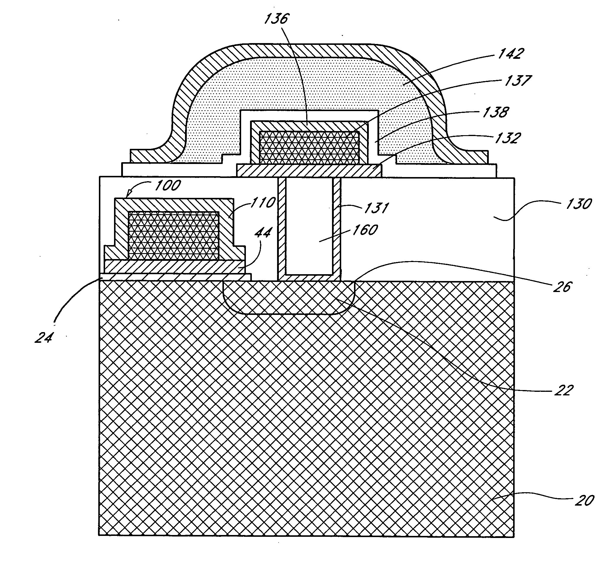
A metal oxide is deposited on a substrate in a semiconductor fabrication metallization process is patterned and subsequently reduced to a more conductive form, such as elemental metal. The metal oxide is reduced by exposure to at least one reducing agent or current that is capable of removing oxygen from the metal oxide. Copper oxide, for example, can be dry etched for patterning prior to reduction to copper metal, and the patterned copper used as an ECD seed layer.

Description

REFERENCE TO RELATED APPLICATON [0001] The present non-provisional application claims the priority benefit of U.S. provisional application No. 60 / 588,844, filed Jul. 15, 2004, which is incorporated herein by reference. The present application is also related to U.S. application Ser. No. 10 / 300,168, filed Nov. 19, 2002, now U.S. Pat. No. 6,887,795, and U.S. application Ser. No. 09 / 975,466, filed Oct. 9, 2001, now U.S. Pat. No. 6,878,628.FIELD OF THE INVENTION [0002] The invention relates generally to methods of metallization in which metal oxide is deposited, etched and subsequently reduced to elemental metal in semiconductor processing. BACKGROUND OF THE INVENTION [0003] When fabricating integrated circuits, layers of insulating, conducting and semiconducting materials are deposited and patterned to produce desired structures. A process of fabricating a semiconductor integrated circuit is roughly divided into the process of forming devices on a substrate and the process of electrica...

Claims


Application Information

Patent Timeline
IPC IPC(8): H01L21/44H01L21/461H01L21/26
CPCH01L21/76823H01L21/76838H01L21/76873H01L29/518H01L27/10861H01L27/10873H01L29/517H01L27/10829H10B12/37H10B12/038H10B12/05
Inventor LI, WEI MIN
Owner ASM INTERNATIONAL
Learn More