

Semiconductor memory device and method for fabricating the same
- Summary
- Abstract
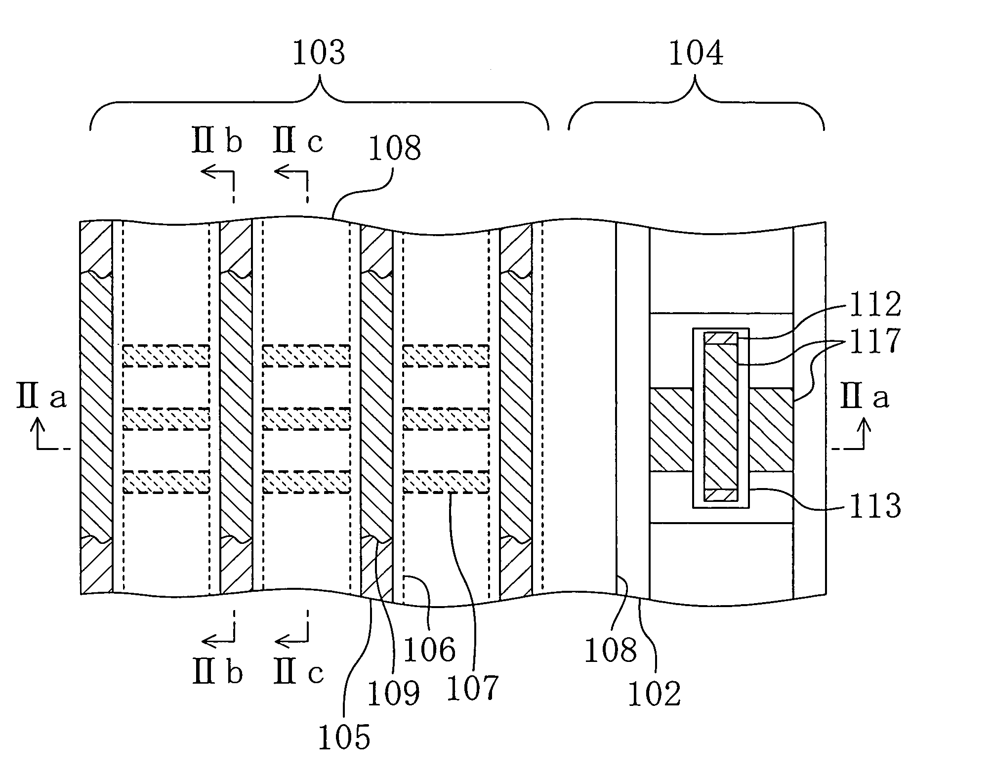
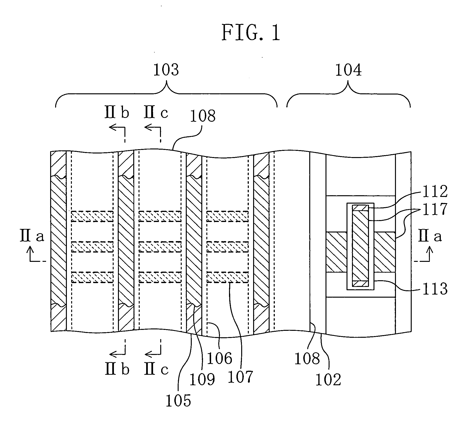
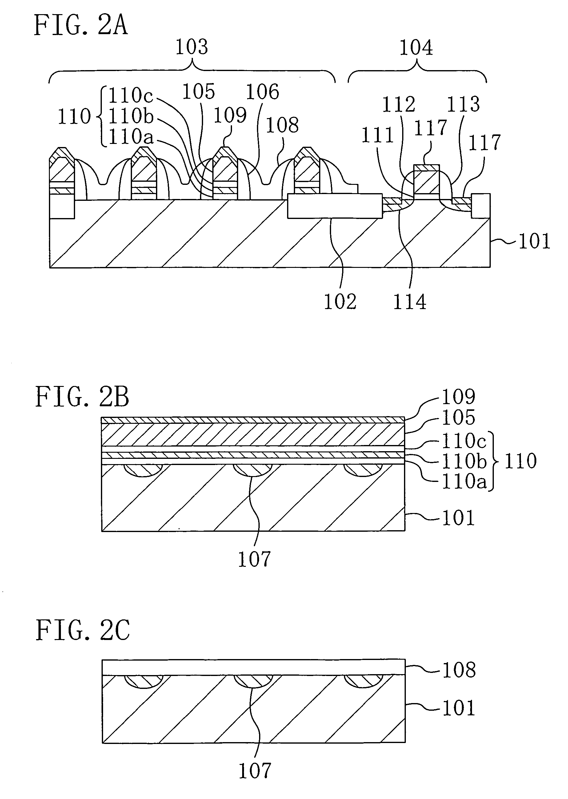
- Description
- Claims
- Application Information
AI Technical Summary
Benefits of technology
Problems solved by technology
Method used
Image

Examples
embodiment 1
Variation 2 of Embodiment 1
[0095] Referring to FIGS. 12A to 12C, a description will be given herein below to a method for fabricating a semiconductor memory device according to a second variation of the first embodiment of the present invention.
[0096] In contrast to the fabrication method according to the first embodiment which has used the atmospheric-pressure CVD as the deposition method for the second insulating film 116 shown in FIGS. 5A to 5C, the fabrication method according to the second variation uses a reverse sputtering process such as argon sputtering.
[0097] Specifically, as shown in FIG. 12A, 12B, and 12C, when the second insulating film 116 composed of the BPSG film is deposited by using a sputtering technology which covers the surface (target surface) of a target material made of silicon oxide containing a phosphorus impurity and a boron impurity for a proper period of time to perform so-called reverse sputtering, the second insulating film 116 having a configuration...
embodiment 2
Variation 2 of Embodiment 2
[0135] Referring to FIGS. 21A to 21C, a description will be given herein below to a method for fabricating a semiconductor memory device according to a second variation of the second embodiment of the present invention.
[0136] In contrast to the fabrication method according to the second embodiment which has used the atmospheric-pressure CVD as the deposition method for the insulating film 215 shown in FIGS. 15A to 15C, the fabrication method according to the second variation uses a reverse sputtering process such as argon sputtering.
[0137] Specifically, as shown in FIG. 15A, 15B, and 15C, when the insulating film 215 made of silicon oxide is deposited by using a sputtering technology which covers the surface (target surface) of a target material made of silicon oxide for a proper period of time to perform so-called reverse sputtering, the insulating film 215 having a configuration which is thinner over the edge portions of the upper surface of each of th...
PUM
 Abstract
Description
Claims
Application Information