

Surface acoustic wave device, surface acoustic wave apparatus, and communications equipment
- Summary
- Abstract
- Description
- Claims
- Application Information
AI Technical Summary
Benefits of technology
Problems solved by technology
Method used
Image

Examples
example
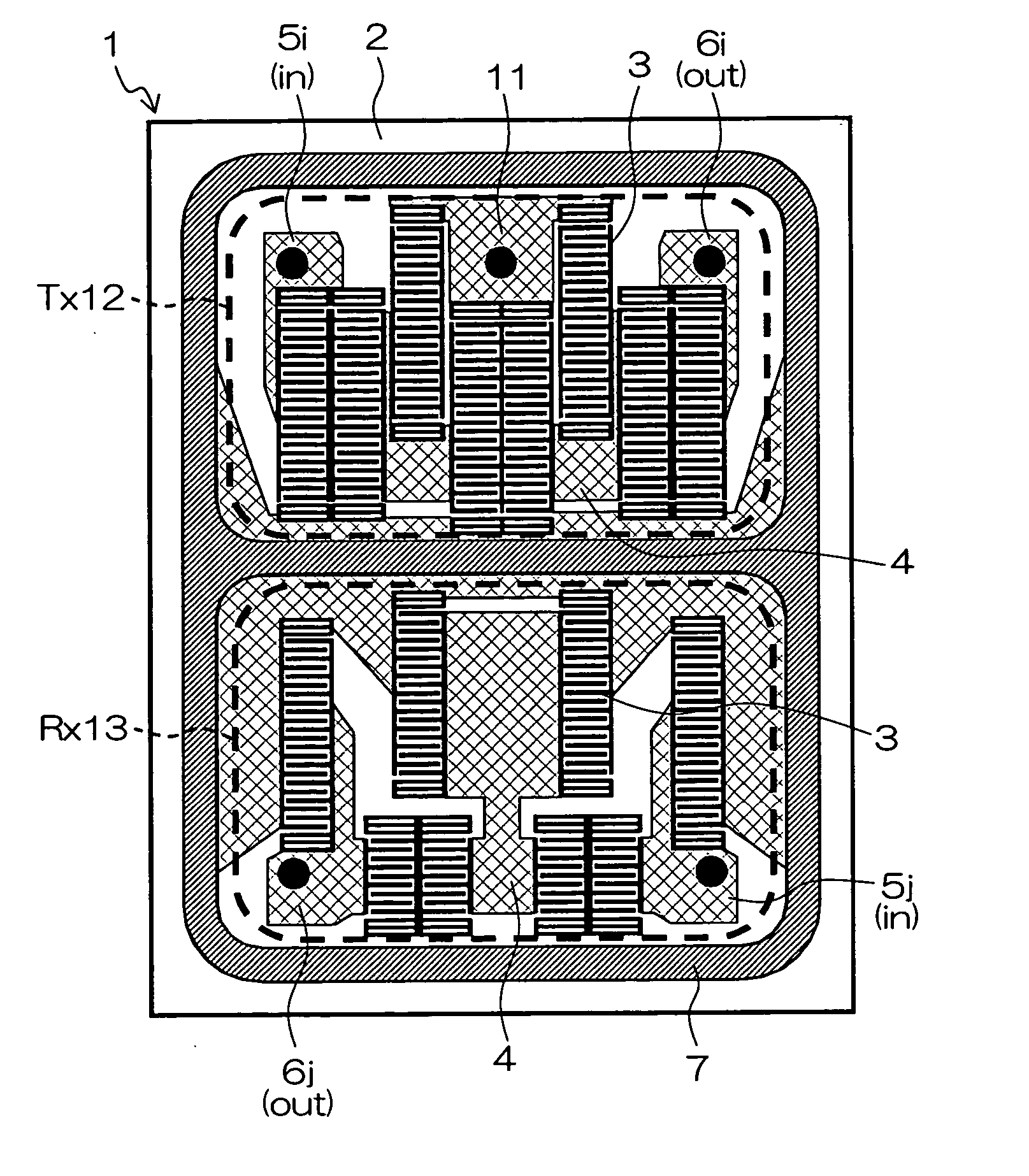
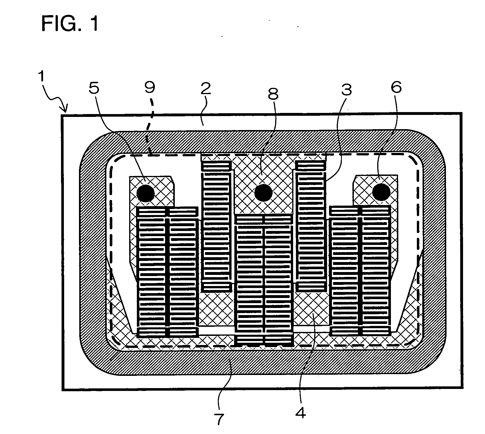
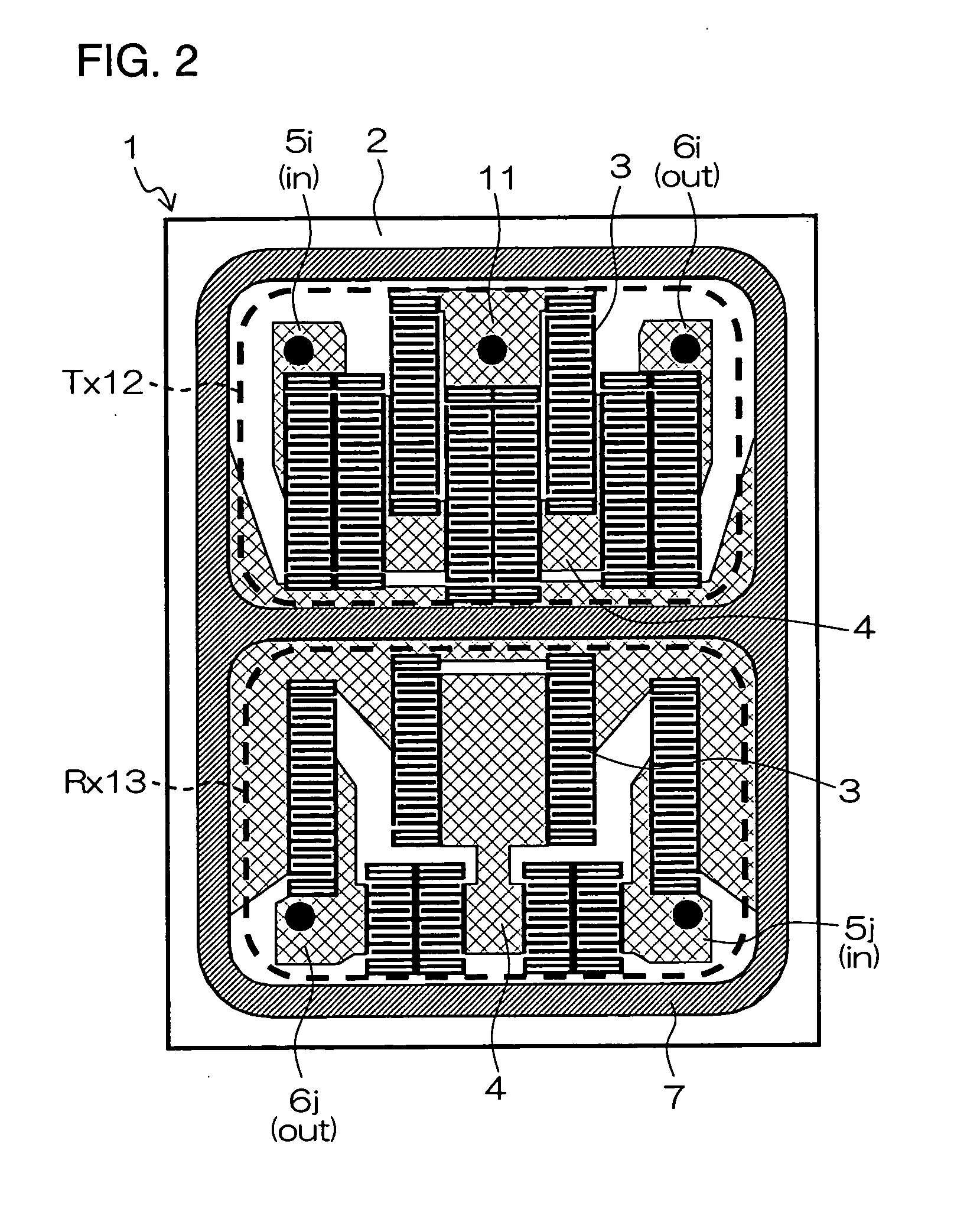
[0173] An example in which a surface acoustic wave filter that is the surface acoustic wave apparatus shown in FIG. 6 is specifically produced by way of trial using the surface acoustic wave device 1A shown in FIG. 7.
[0174] The other main surface of a piezoelectric substrate 2 and one main surface of a second substrate 21 were joined using a vitreous member composed of quartz glass as an adhesive layer 23 or a piezoelectric substrate 2 (125 μm in thickness) of a piezoelectric member composed of a 38.7-degree Y-cut X-propagation lithium tantalate (LT) single crystal. Used as the second substrate 21 was a quartz substrate having a dielectric constant εr of 4.5. The dielectric constant 4.5 was lower than the dielectric constant 42.7 of a lithium tantalate single crystal substrate.
[0175] On one main surface of the piezoelectric substrate 2, four conductor layers respectively composed of Ti, Al-1 mass percent Cu, Ti, and Al-1 mass percent Cu were deposited in this order on the side of ...
PUM
 Abstract
Description
Claims
Application Information