Stacked chip electronic package having laminate carrier and method of making same

Inactive Publication Date: 2006-02-02
TTM TECH NORTH AMERICA LLC
View PDF31 Cites 42 Cited by
  • Summary
  • Abstract
  • Description
  • Claims
  • Application Information

AI Technical Summary

Benefits of technology

[0019] It is, therefore, a primary object of the present invention to enhance the art of chip carriers including more

Problems solved by technology

The use of a multi-layered interconnect structure such as an organic, laminate chip carrier for interconnecting a semiconductor chip to a printed circuit board in an electronic package introduces many challenges, one of which is the reliability of the connection joints between the semiconductor chip and the organic chip carrier and another of which is the reliability of the connection joints between the organic chip carrier and the printed circuit board.
Similarly, the industry standard ball grid array (BGA) interconnections between the organic chip carrier and printed circuit board can also exhibit high stress during operation.
Significant reliability concerns may then become manifest by failure of the connections or even failure of the integrity of the semiconductor chip (chip cracking).
These reliability concerns significantly inhibit design flexibility.
These limitations may limit the electrical performance advantages of the organic electronic package or add significant cost to the electronic package.
The use of ceramic, however, poses many problems, a primary one of which is handling.
Ceramic is a relatively brittle material capable of cracking and chipping if handled improperly, especially during manufacture and shipping.
Ceramic is also a relatively difficult material to process, especially to the multi-depth level where several individual layers of insulative and interconnecting conductive materials are needed to satisfy many operational r

Method used


Image

  • Stacked chip electronic package having laminate carrier and method of making same
  • Stacked chip electronic package having laminate carrier and method of making same
  • Stacked chip electronic package having laminate carrier and method of making same

Examples


Example

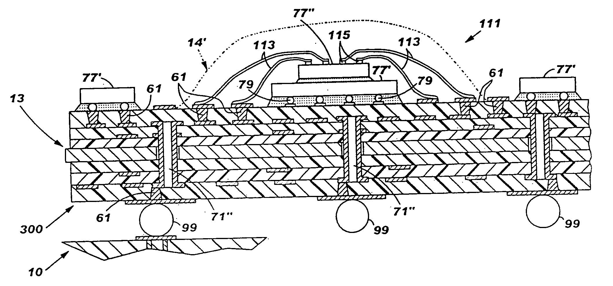
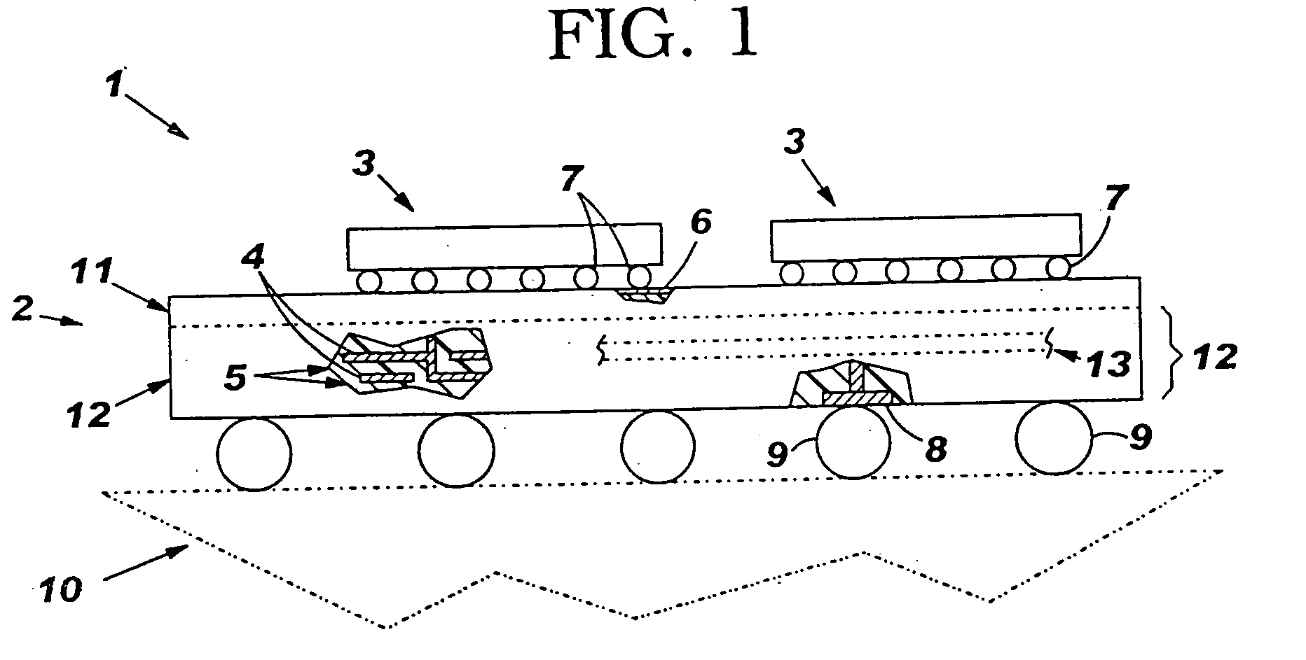
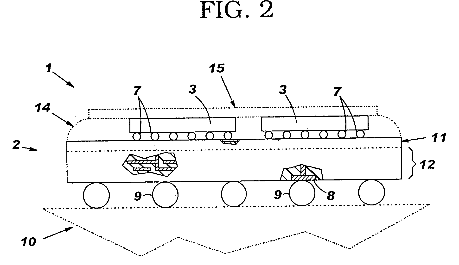
[0043] For a better understanding of the present invention, together with other and further objects, advantages and capabilities thereof, reference is made to the following disclosure and appended claims in connection with the above-described drawings. It is understood that like numerals will be used to indicate like elements from FIG. to FIG.

[0044] As stated above, the term “high speed” as used herein is meant signals of high frequency. Examples of such signal frequencies attainable for the multilayered chip carriers and circuitized substrates (e.g., PCBs) defined herein and as produced using the methods taught herein include those within the range of from about 3.0 to about 10.0 gigabits per second (GPS). These examples are not meant to limit this invention, however, because frequencies outside this range, including those higher, are attainable. As further understood from the following, the carrier products produced herein may be formed of at least two separate multilayered porti...


PUM

PropertyMeasurementUnit
Thicknessaaaaaaaaaa
Electrical conductivityaaaaaaaaaa
Electrical conductoraaaaaaaaaa

Abstract

A multi-chip electronic package which utilizes an organic, laminate chip carrier and a pair of semiconductor chips positioned on an upper surface of the carrier in a stacked orientation. The organic, laminate chip carrier is comprised of a plurality of conductive planes and dielectric layers and couples one or both of the chips to underlying conductors on the bottom surface thereof. The carrier may include a high-speed portion to assure high-frequency connection between the semiconductor chips and may also include an internal capacitor and/or thermally conductive member for enhanced operational capabilities. The first chip, e.g., an ASIC chip, is solder bonded to the carrier while the second chip, e.g., a memory chip, is secured to the first chip's upper surface and coupled to the carrier using a plurality of wirebond connections.

Description

CROSS-REFERENCE TO CO-PENDING APPLICATION [0001] This application is a continuation-in-part of application Ser. No. 10 / 394,107, filed Mar. 24, 2003 and entitled “Multi-Chip Electronic Package Having Laminate Carrier” (inventors: L Fraley et al), which is a continuation-in-part of application Ser. No. 10 / 354,000, filed Jan. 30, 2003, and entitled, “High Speed Circuit Board And Method For Fabrication” (inventors: B. Chan et al).TECHNICAL FIELD [0002] The present invention relates, in general, to an electronic package for mounting of integrated circuits, and in particular, to an organic, multi-layered laminated interconnect structure for use in such a package. BACKGROUND OF THE INVENTION [0003] Organic laminate substrates, for example printed circuit boards and chip carriers, have been and continue to be developed for many applications. One such chip carrier is sold under the name HyperBGA by the assignee of this invention. (HyperBGA is a registered trademark of Endicott Interconnect T...

Claims


Application Information

Patent Timeline
IPC IPC(8): H05K7/06H01L23/48H01L23/34H01L23/12H01L23/14H01L23/31H01L23/498H01L23/538H01L25/04H01L25/065H01L25/07H01L25/18H05K1/02H05K1/11H05K3/46
CPCH01L21/563H01L23/145H01L23/3128H01L23/49822H01L23/5383H01L25/0652H01L25/0655H01L25/18H01L25/50H01L2224/16225H01L2224/16237H01L2224/32145H01L2224/48091H01L2224/48227H01L2224/48472H01L2224/73204H01L2224/73253H01L2224/73265H01L2924/01057H01L2924/01078H01L2924/12044H01L2924/14H01L2924/1433H01L2924/15311H01L2924/16195H01L2924/19041H01L2924/3011H01L2924/3025H05K1/024H05K1/113H05K3/4623H05K3/4688H05K2201/09536H05K2201/096H05K2203/061H01L24/48H01L2924/01019H01L2225/06558H01L2224/32225H01L2224/32245H01L2924/19105H01L2924/12041H05K2201/10378H01L2224/16235Y10T29/49155Y10T29/49144Y10T29/49133H01L2924/00014H01L2924/00H01L2924/00012H01L2924/12042H01L24/73H01L2924/181H01L2224/05599H01L2224/45099H01L2224/85399H01L2924/18161H01L2224/45015H01L2924/207
Inventor FRALEY, LAWRENCE R.MARKOVICH, VOYA
Owner TTM TECH NORTH AMERICA LLC
Why Eureka
Try Eureka