Metal capacitor stacked with a MOS capacitor to provide increased capacitance density

a technology of metal capacitors and mos capacitors, applied in capacitors, semiconductor devices, semiconductor/solid-state device details, etc., can solve the problems of mos capacitors not making use of the space above the capacitor for creating additional capacitance, capacitor devices consume a large part of the total area of an integrated circuit, and each of the three types of capacitors has substantial limitations when used alone, so as to achieve effective increase the capacitance density and increase the processing cost

Inactive Publication Date: 2006-02-02
BELL SEMICON LLC
View PDF15 Cites 68 Cited by
  • Summary
  • Abstract
  • Description
  • Claims
  • Application Information

AI Technical Summary

Benefits of technology

[0009] The present invention addresses the above-identified need by providing a novel design for effectively increasing capacitance density without increasing processing costs. The design achieves this by stacking vertically MOS capacitors with metal interconnect capacitors and providing interconnection in such a way as to combine capacitance densities.

Problems solved by technology

In many cases, capacitor devices consume a large part of an integrated circuit's total area.
Each of the three types of capacitors has substantial limitations when used alone.
However, MOS capacitors do not make use of the space above the capacitor for creating additional capacitance.
Moreover, capacitors created by metal interconnects suffer from low capacitance and, as a result, by themselves are not an area-efficient way to create capacitive devices on integrated circuits.
Likewise, MIM capacitors have low capacitance density, approximately 1 fF / μm2, and, as a result, are also not area efficient.
Cost of implementation, therefore, may be very high.

Method used


Image

  • Metal capacitor stacked with a MOS capacitor to provide increased capacitance density
  • Metal capacitor stacked with a MOS capacitor to provide increased capacitance density
  • Metal capacitor stacked with a MOS capacitor to provide increased capacitance density

Examples


Embodiment Construction

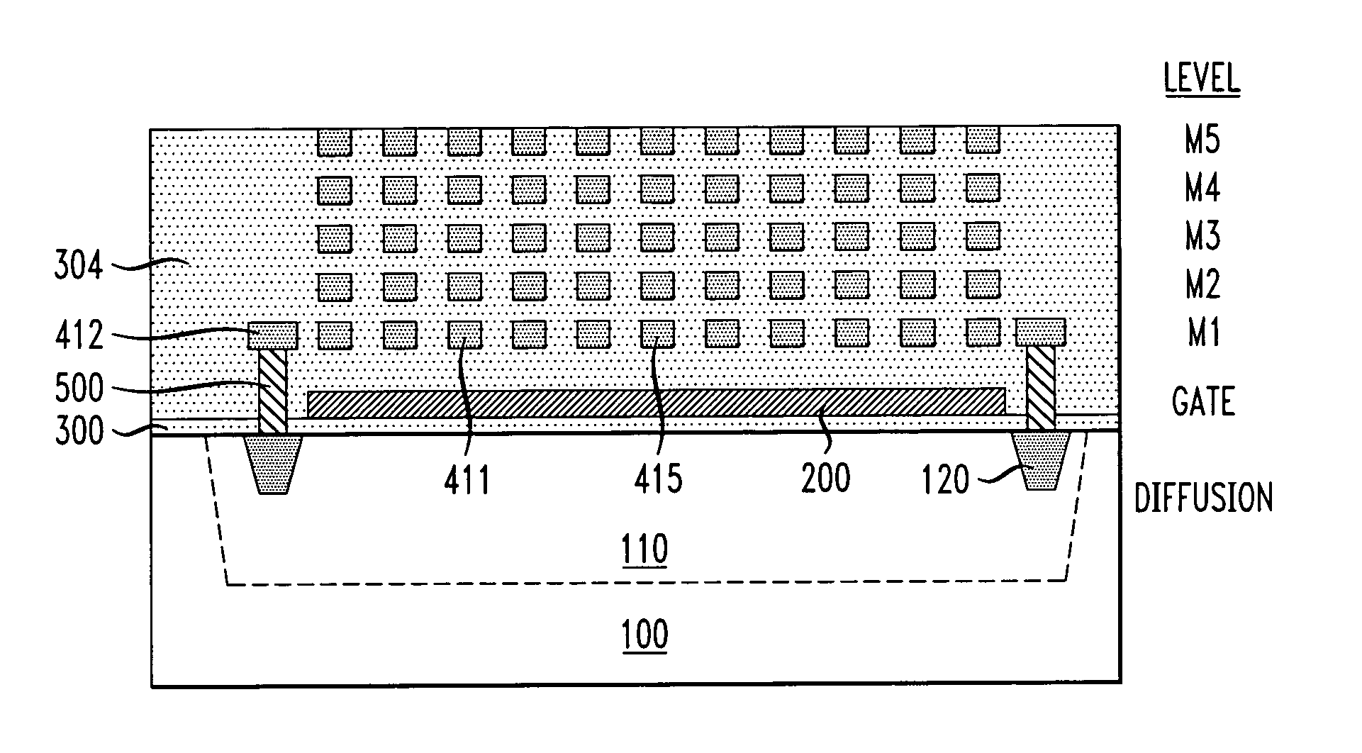
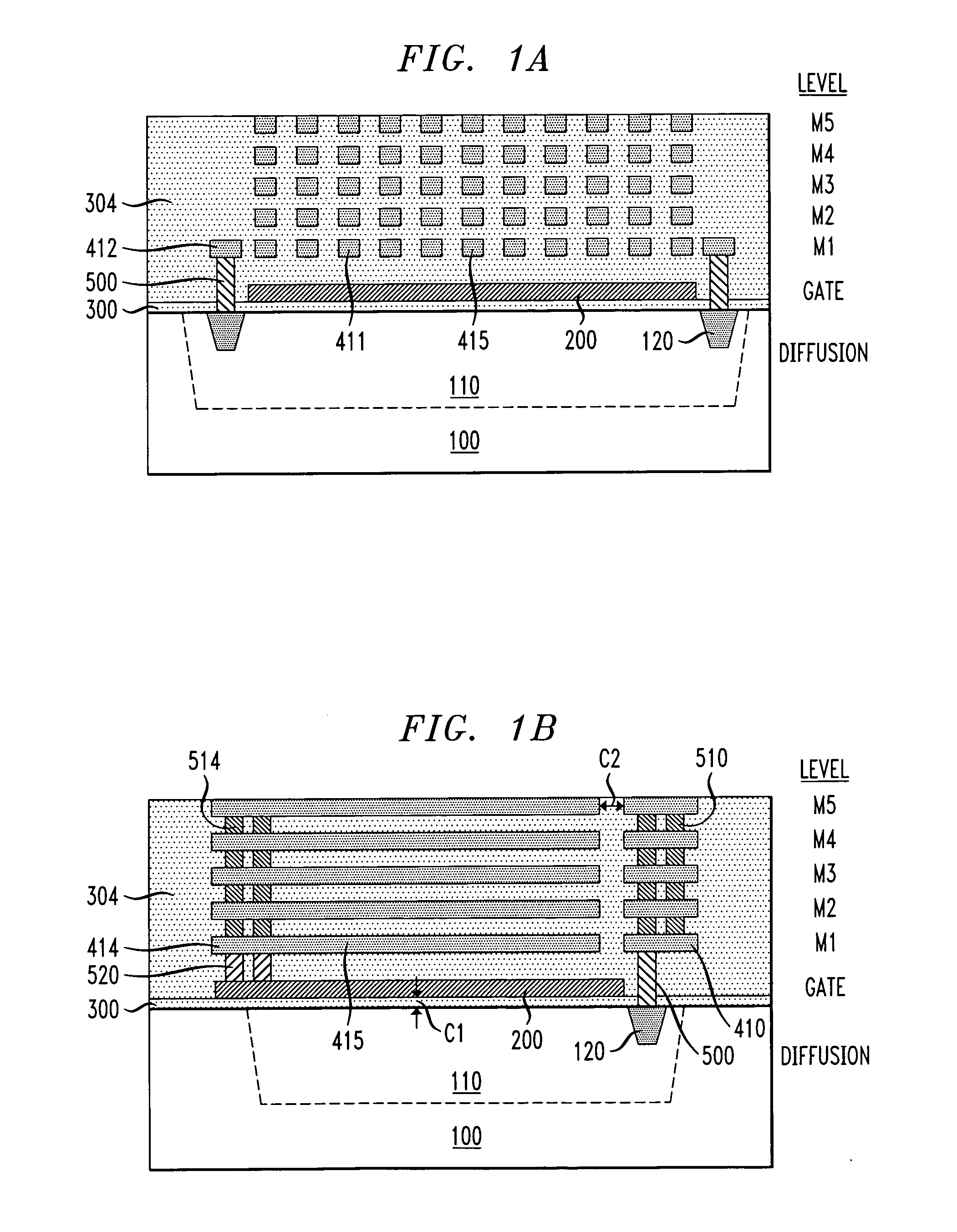
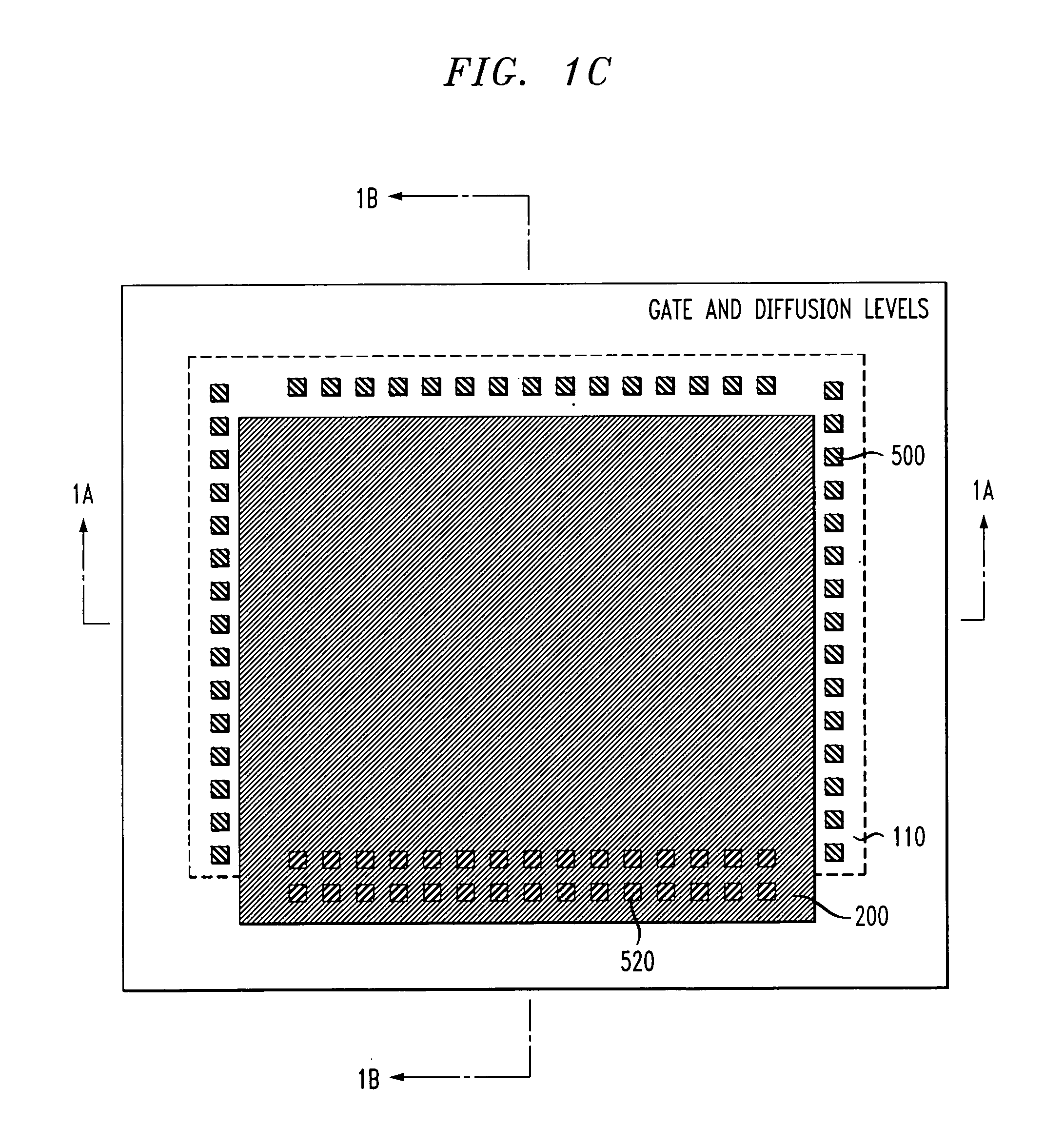
[0021] The vertical direction is defined herein as that direction normal to the surface of the substrate.

[0022] The horizontal direction is defined herein as that direction parallel to the surface of the substrate.

[0023] The term “level” is defined herein as a plane parallel to the surface of the substrate containing one or more patterned features.

[0024] The term “capacitance density” is defined herein as capacitance per unit area of the integrated circuit.

[0025] The present invention will be illustrated below in conjunction with an illustrative embodiment of an on-chip capacitive device. It should be understood, however, that the invention is not limited to the particular circuitry arrangements of the illustrative embodiment. For example, those skilled in the art will recognize that the conductivity types of the devices in a given circuit design may be reversed, e.g., n-type devices may be replaced by p-type devices. These and other modifications to the illustrative embodiment ...


PUM


Abstract

An on-chip capacitive device comprises a semiconductor substrate, a MOS capacitor formed on the semiconductor substrate, and a metal interconnect capacitor formed at least in part in a region above the MOS capacitor. The MOS capacitor and the metal interconnect capacitor are connected in parallel to form a single capacitive device. The capacitance densities of the MOS capacitor and the metal interconnect capacitor are, thereby, combined. Advantageously, significant capacitance density gains can be achieved without additional processing steps.

Description

FIELD OF THE INVENTION [0001] This invention relates generally to integrated circuits, and more specifically to capacitive devices in integrated circuits. BACKGROUND OF THE INVENTION [0002] As analog circuits have been integrated with digital circuits on Complementary-Metal-Oxide-Semiconductor (CMOS) integrated circuits, the capacitor has come to dominate analog circuit design. In many cases, capacitor devices consume a large part of an integrated circuit's total area. As a result, decreasing the size of capacitor devices will allow an integrated circuit to be smaller, and, thereby, allow the integrated circuit to be produced more cost effectively. [0003] Integrated circuits typically contain one or more of three types of capacitors. The first type is a Metal-Oxide-Semiconductor (MOS) capacitor. In such a device, the near-surface region of a doped semiconductor substrate acts as one terminal of the capacitor. The gate conductor is used as the other terminal, and the gate oxide acts ...

Claims


Application Information

Patent Timeline
Patent Type & Authority Applications(United States)
IPC IPC(8): H01L21/20
CPCH01L23/5223H01L27/0207H01L27/0805H01L28/86H01L2924/0002H01L2924/00
Inventor HE, CANZHONGSCHULER, JOHN A.SHARPE, JOHN M.VUONG, HONG-HA
Owner BELL SEMICON LLC
Why Eureka
Try Eureka