Method of reducing the surface roughness of a semiconductor wafer

Inactive Publication Date: 2006-02-02
S O I TEC SILICON ON INSULATOR THECHNOLOGIES
View PDF35 Cites 10 Cited by
  • Summary
  • Abstract
  • Description
  • Claims
  • Application Information

AI Technical Summary

Benefits of technology

[0024] The invention thus provides an improved method of reducing the surface roughness of a wafe

Problems solved by technology

However, such treatment does not decrease the roughness of wafers down to the level of the above-mentioned specifications.
But such techniques lead to a method that is lengthy and complex.
However, if a defect concentration gradient that increases towards the free surface of the wafer exists, this second method can also abrade the wafer down to a zone that presents an acceptable concentration of defects.
But this second known method can compromise the uniformity of the free surface of the wafer.
This drawback is worsened when a large amount of polishing is performed on the surface of the wafer, as would be necessary to reach the roughness levels mentioned above.
Although this first variant can present certain advantages, the aggressive nature of the mixture of gases of the atmosphere limits the use of such a method, and elements other than the free surface of the wafer may be exposed to the action thereof (the face of the wafer or the structure to which it is bonded that faces away from the free surface of the wafer may also be detrimentally affected and sometimes also the annealing chamber may be detr

Method used


Image

  • Method of reducing the surface roughness of a semiconductor wafer
  • Method of reducing the surface roughness of a semiconductor wafer
  • Method of reducing the surface roughness of a semiconductor wafer

Examples


Embodiment Construction

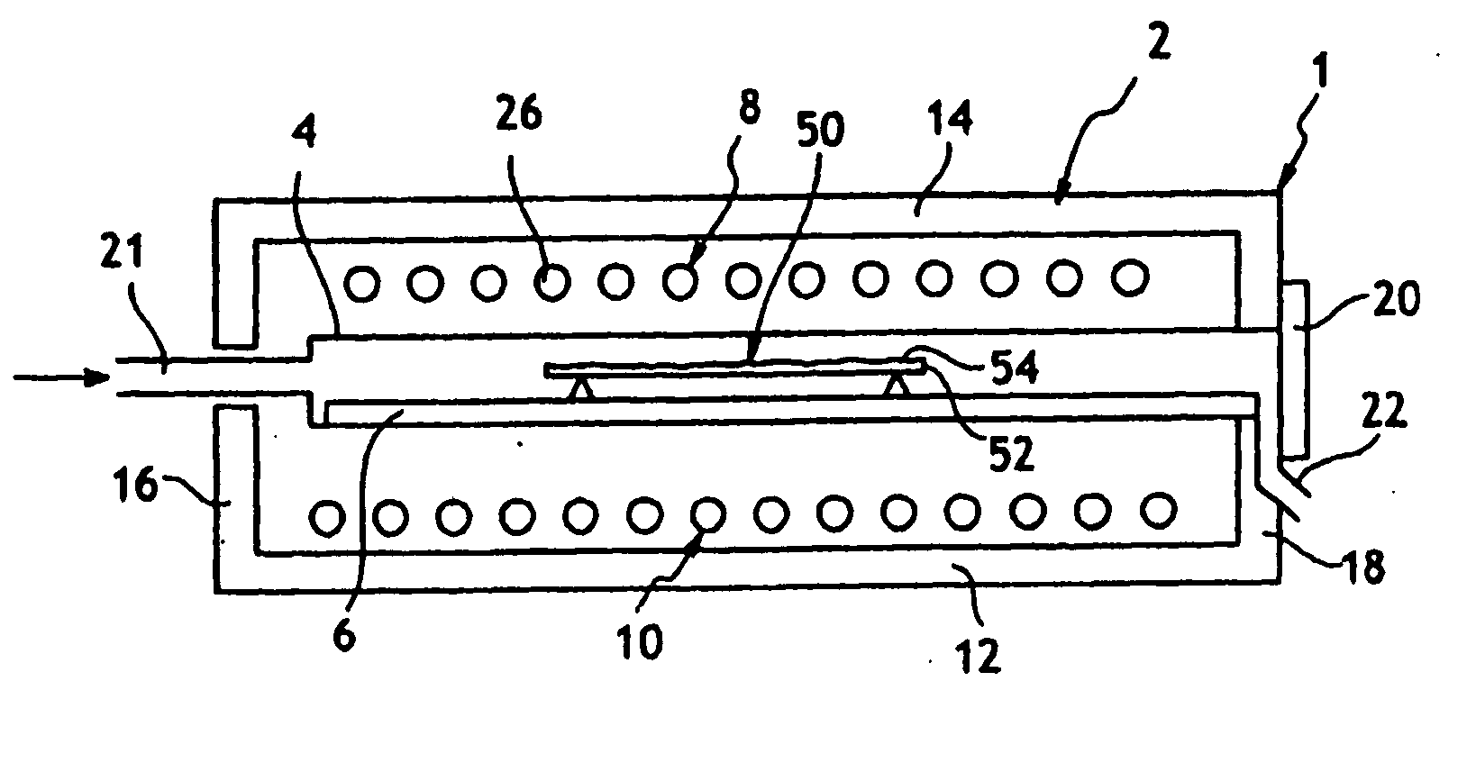
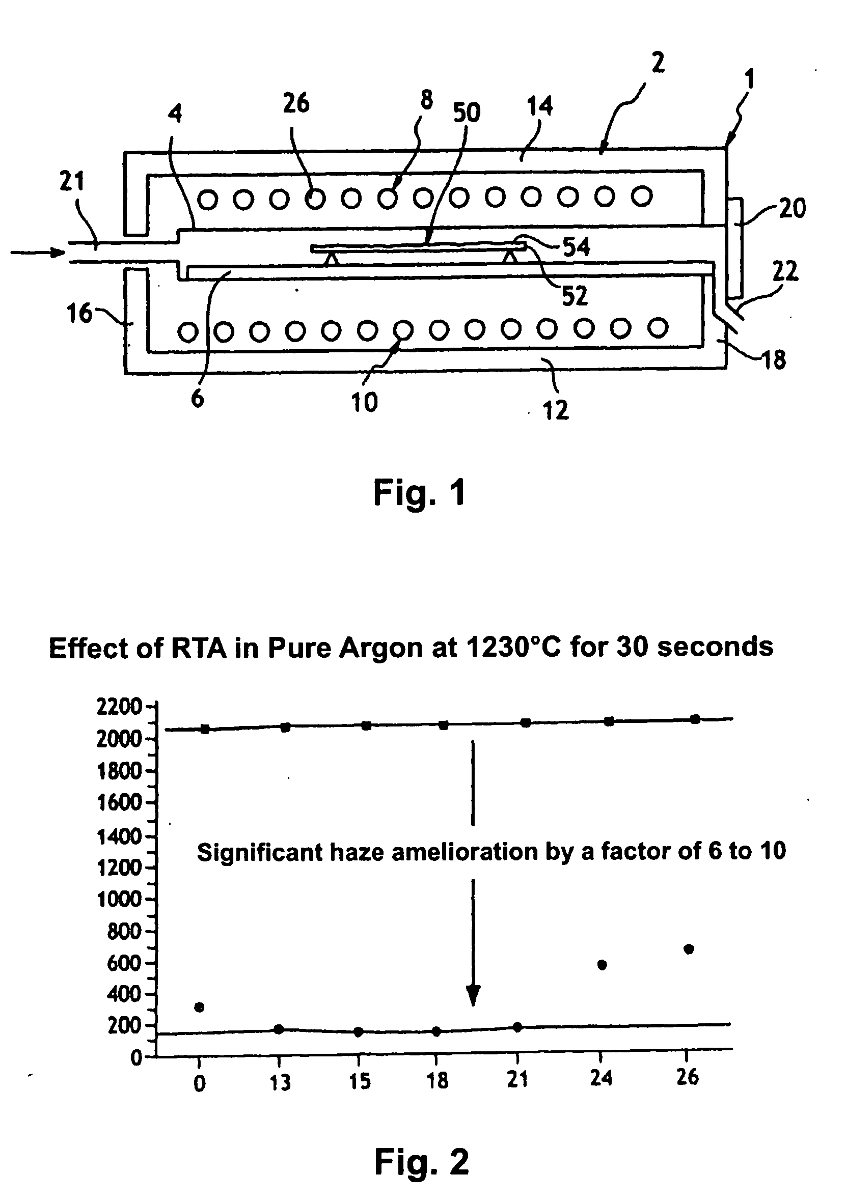
[0033]FIG. 1 is a non-limiting example of an annealing chamber 1 that enables the invention to be implemented. The chamber is used to implement an annealing stage under a pure argon atmosphere using the RTA technique.

[0034] In this implementation, the chamber 1 preferably includes an enclosure 2, a reactor 4, a substrate-carrier tray 6, two arrays of halogen lamps 8, 10, and two opposed pairs of side lamps (not shown). The enclosure 2 also includes a bottom wall 12, a top wall 14, and two side walls 16,18 situated at respective longitudinal ends of the enclosure 2. One of the side walls 16,18 includes a gate 20. The reactor 4 preferably includes a quartz tube extending longitudinally between the two side walls 16, 18. A gas inlet 21 and a gas outlet 22 are provided at the respective side walls 16 and 18. The gas outlet 22 is preferably situated in the side wall 18 that has the gate 20. The arrays 8,10 of halogen lamps are preferably situated above and below the reactor 4, respectiv...


PUM

PropertyMeasurementUnit
Temperatureaaaaaaaaaa

Abstract

A method for reducing the roughness of a free surface of a semiconductor wafer that includes establishing a first atmosphere in an annealing chamber, replacing the first atmosphere with a second atmosphere that includes a gas selected to and in an amount to substantially eliminate or reduce pollutants on a wafer, and exposing the free surface of the wafer to the second atmosphere to substantially eliminate or reduce pollutants thereon. The second atmosphere is then replaced with a third atmosphere that includes pure, and rapid thermal annealing is performed on the wafer exposed to the third atmosphere in the annealing chamber to substantially reduce the roughness of the free surface of the wafer.

Description

CROSS-REFERENCE TO RELATED APPLICATIONS [0001] This application is a continuation-in-part of U.S. application Ser. No. 10 / 750,443, filed on Dec. 30, 2003, which is a continuation of International Application PCT / FR02 / 02341, filed on Jul. 4, 2002. This application is also a continuation-in-part of International Application PCT / IB2003 / 06380, filed on Dec. 3, 2003. The entire contents of each of the above-referenced applications are expressly incorporated herein by reference thereto.FIELD OF THE INVENTION [0002] The present invention relates to a method for treating a semiconductor wafer. More particularly, the invention relates to treating a surface of the semiconductor wafer by annealing. BACKGROUND OF THE INVENTION [0003] The present invention generally relates to the surface treatment of semiconductor materials, and in particular to treating substrates for fabricating components for microelectronic and / or optoelectronic applications. More precisely, the invention concerns a method ...

Claims


Application Information

Patent Timeline
IPC IPC(8): H01L21/20H01L21/02H01L21/26H01L21/302H01L21/324H01L21/762H01L27/12
CPCH01L21/302H01L21/76254H01L21/324H01L21/3247
Inventor NEYRET, ERICECARNOT, LUDOVICARENE, EMMANUEL
Owner S O I TEC SILICON ON INSULATOR THECHNOLOGIES
Why Eureka
Try Eureka