Methods of enabling polysilicon gate electrodes for high-k gate dieletrics

a polysilicon and gate electrode technology, applied in the field of complementary transistors, can solve the problems of large shift in the choice of a material with the appropriate work function as the gate electrode remains a challenge, and the transistor vsub>t /sub>will shift larg

Active Publication Date: 2006-02-09
MICRON TECH INC
View PDF19 Cites 25 Cited by
  • Summary
  • Abstract
  • Description
  • Claims
  • Application Information

AI Technical Summary

Benefits of technology

[0008] Exemplary implementations of the present invention include complementary transistors and methods of forming the complementary transistors on a semiconductor assembly by optionally forming an interfacial oxide, such as SiO2 or oxy-nitride, for electron or hole mobility, to overlay a semiconductor substrate which will be conductively doped for PMOS and NMOS regions. Then a dielectric possessing a high dielectric constant of least seven or greater (also referred to herein as a high-k dielectric) is deposite

Problems solved by technology

However, choosing a material with the appropriate work function as a gate electrode is still a challenge.
However, applying this case in a PMOS device, a large shift in the transistor Vt will occur due to the Hafnium-Silicon bonds still pinning the Fermi-Level of the polysilicon near the c

Method used


Image

  • Methods of enabling polysilicon gate electrodes for high-k gate dieletrics
  • Methods of enabling polysilicon gate electrodes for high-k gate dieletrics
  • Methods of enabling polysilicon gate electrodes for high-k gate dieletrics

Examples


Embodiment Construction

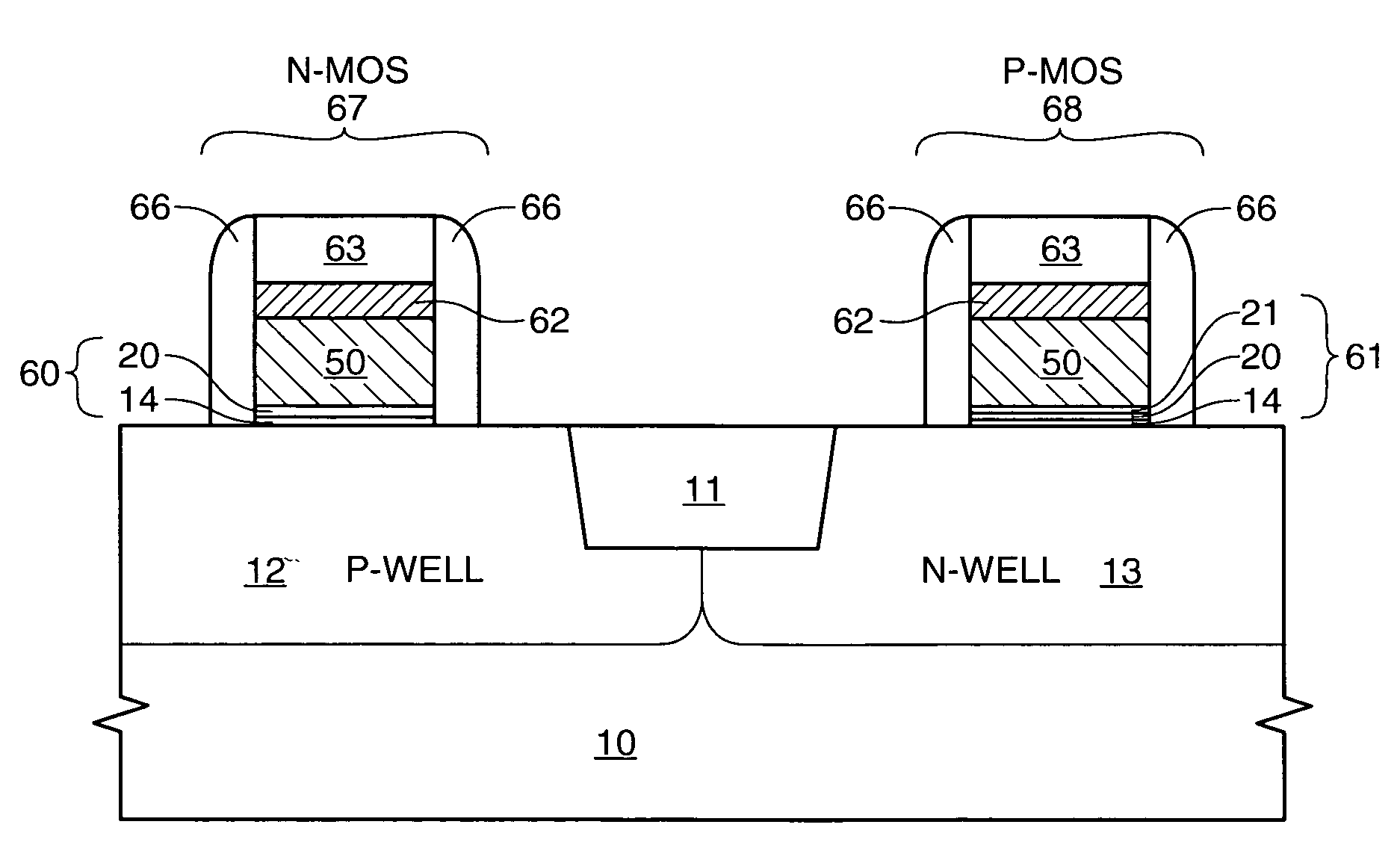
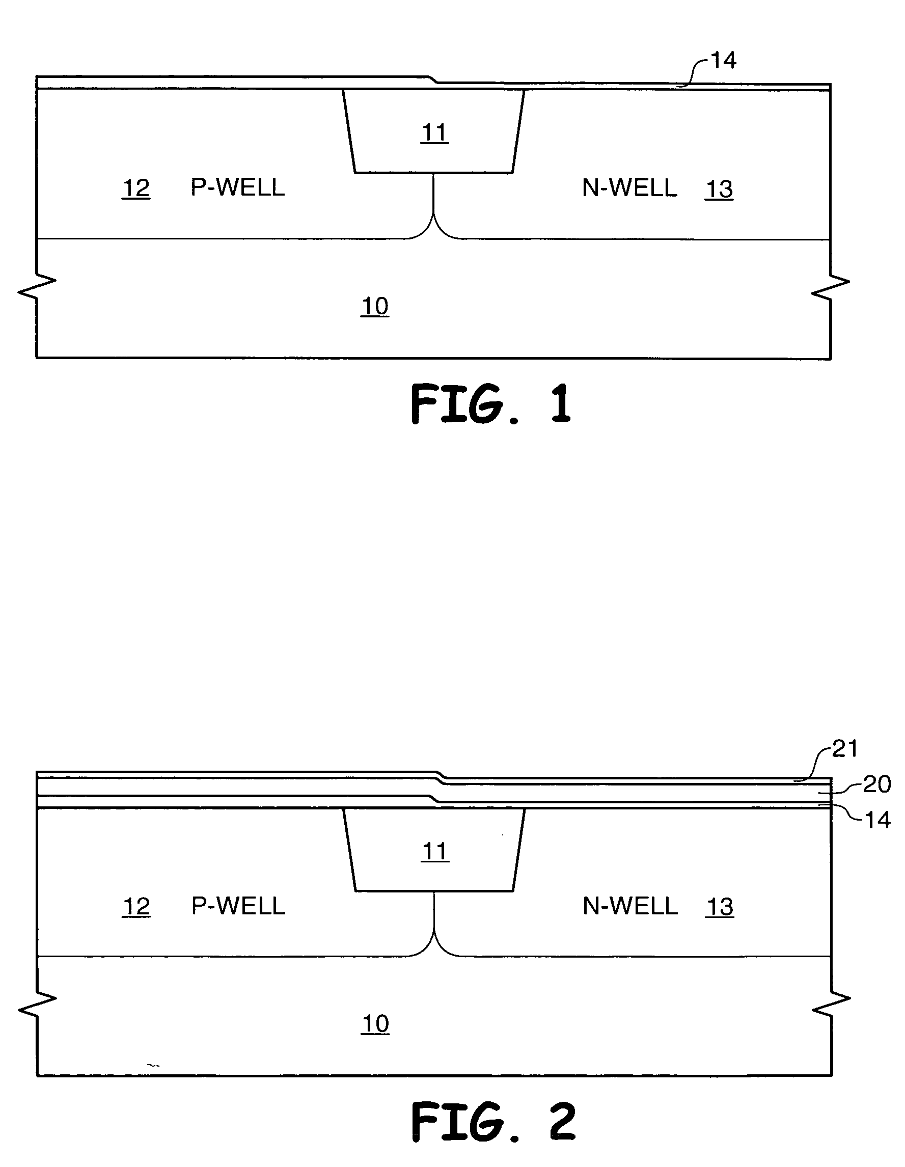
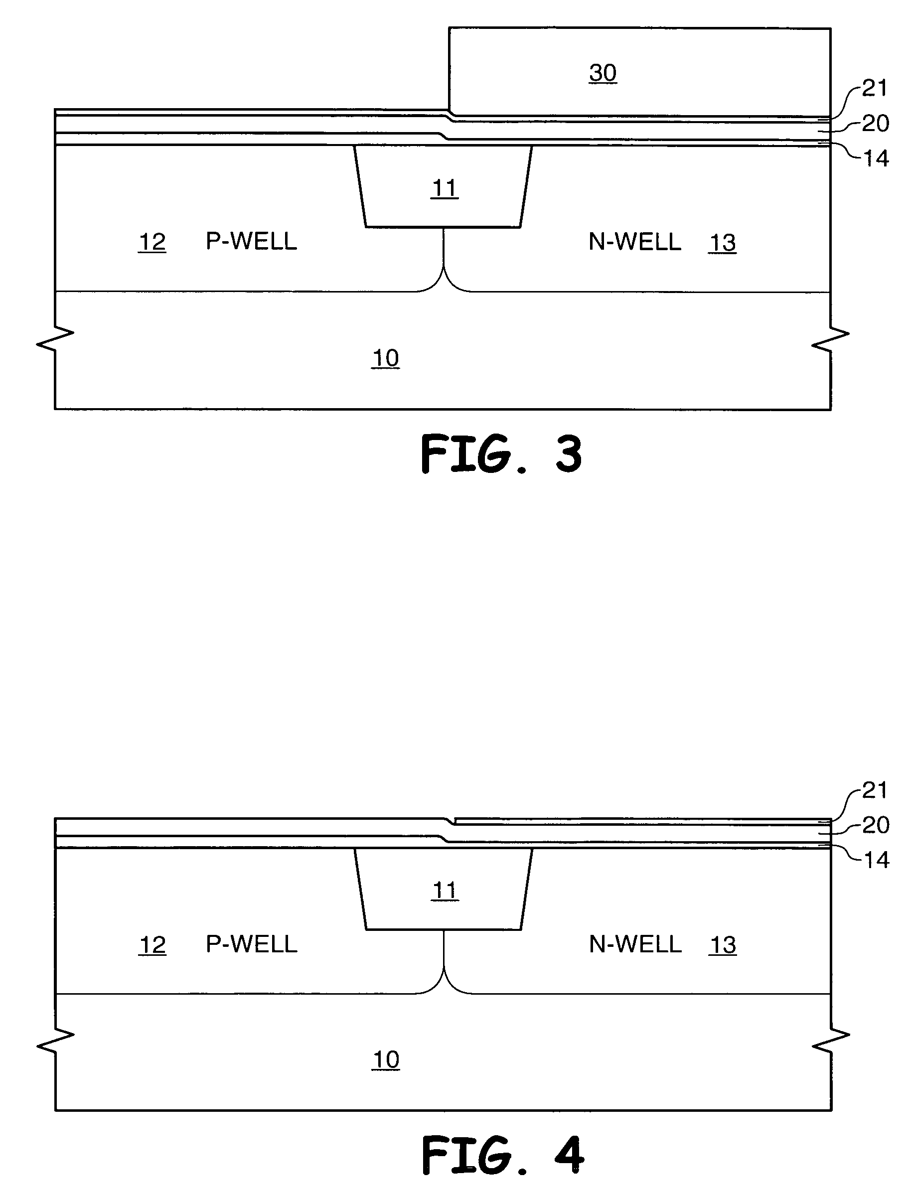
[0016] The following exemplary implementations are in reference to complementary transistors and the formation thereof. While the concepts of the present invention are conducive to transistor structures for semiconductor memory devices, the concepts taught herein may be applied to other semiconductor devices that would likewise benefit from the use of the process disclosed herein. Therefore, the depictions of the present invention in reference to transistor structures for semiconductor memory devices are not meant to so limit the extent to which one skilled in the art may apply the concepts taught hereinafter.

[0017] In the following description, the terms “wafer” and “substrate” are to be understood as a semiconductor-based material including silicon, silicon-on-insulator (SOI) or silicon-on-sapphire (SOS) technology, doped and undoped semiconductors, epitaxial layers of silicon supported by a base semiconductor foundation, and other semiconductor structures. Furthermore, when refe...


PUM


Abstract

Complementary transistors and methods of forming the complementary transistors on a semiconductor assembly are described. The transistors are formed with an optional interfacial oxide, such as SiO2 or oxy-nitride, to overlay a semiconductor substrate which will be conductively doped for PMOS and NMOS regions. Then a dielectric possessing a high dielectric constant of least seven or greater (also referred to as a high-k dielectric) is deposited on the interfacial oxide. The high-k dielectric is covered with a thin monolayer of metal oxide (i.e., aluminum oxide, Al2O3) that is removed from the NMOS regions, but remains in the PMOS regions. The resulting NMOS transistor diffusion regions contain predominately metal to silicon bonds that create predominately Fermi level pinning near the valence band while the resulting PMOS transistor diffusion regions contain metal to silicon bonds that create predominately Fermi level pinning near the conduction band.

Description

FIELD OF THE INVENTION [0001] This invention relates to semiconductor devices and fabrication processes thereof. The invention particularly relates to complementary transistors and a method to fabricate the complementary transistors that utilize transistor gate dielectric materials possessing a high dielectric constant. BACKGROUND OF THE INVENTION [0002] Complementary Metal Oxide Semiconductor (CMOS) devices are dominated by n-channel (NMOS) and p-channel (PMOS) transistor structures. Various physical characteristics of each type of transistor determine the threshold voltage (Vt) that must be overcome to invert the channel region and cause a given transistor to conduct majority carriers (either by electrons movement in an NMOS device or by hole movement in a PMOS device). [0003] One of the controlling physical characteristics is the work function of the material used to form the gate electrode of the transistor device. In semiconductor devices, such as a Dynamic Random Access Memory...

Claims


Application Information

Patent Timeline
IPC IPC(8): H01L21/8238H01L29/76
CPCH01L21/823857H01L21/823842
Inventor WEIMER, RONALD A.
Owner MICRON TECH INC
Why Eureka
Try Eureka