Method of controlling crystal surface morphology using metal adsorption

a technology of crystal surface and metal adsorption, which is applied in the direction of crystal growth process, after-treatment details, nuclear engineering, etc., can solve the problems of inability to control the atomic step to a desired form, the migration direction and width of the atomic steps cannot be accurately controlled, and the crystal surface morphology cannot be controlled

Inactive Publication Date: 2006-02-16
SAMSUNG ELECTRONICS CO LTD
View PDF8 Cites 0 Cited by
  • Summary
  • Abstract
  • Description
  • Claims
  • Application Information

AI Technical Summary

Benefits of technology

[0010] Embodiments of the present invention may provide a method of controlling the morphology of a surfac

Problems solved by technology

However, there is no attempt to control the crystal surface morphology so as to form the surface of the crystal, such as Si or Ge, GaAs, having a specific form of an atomic step structure.
According to this method, a clean silicon wafer surface at an atomic level is obtained, but it is impossible to control the atomic step to a desired form.
In this method, the atomic steps of the silicon crystal surface general

Method used


Image

  • Method of controlling crystal surface morphology using metal adsorption
  • Method of controlling crystal surface morphology using metal adsorption
  • Method of controlling crystal surface morphology using metal adsorption

Examples


Embodiment Construction

[0021] Hereinafter, a method of controlling the crystal surface morphology according to an embodiment of the present invention will be described in more detail with reference to the attached drawings.

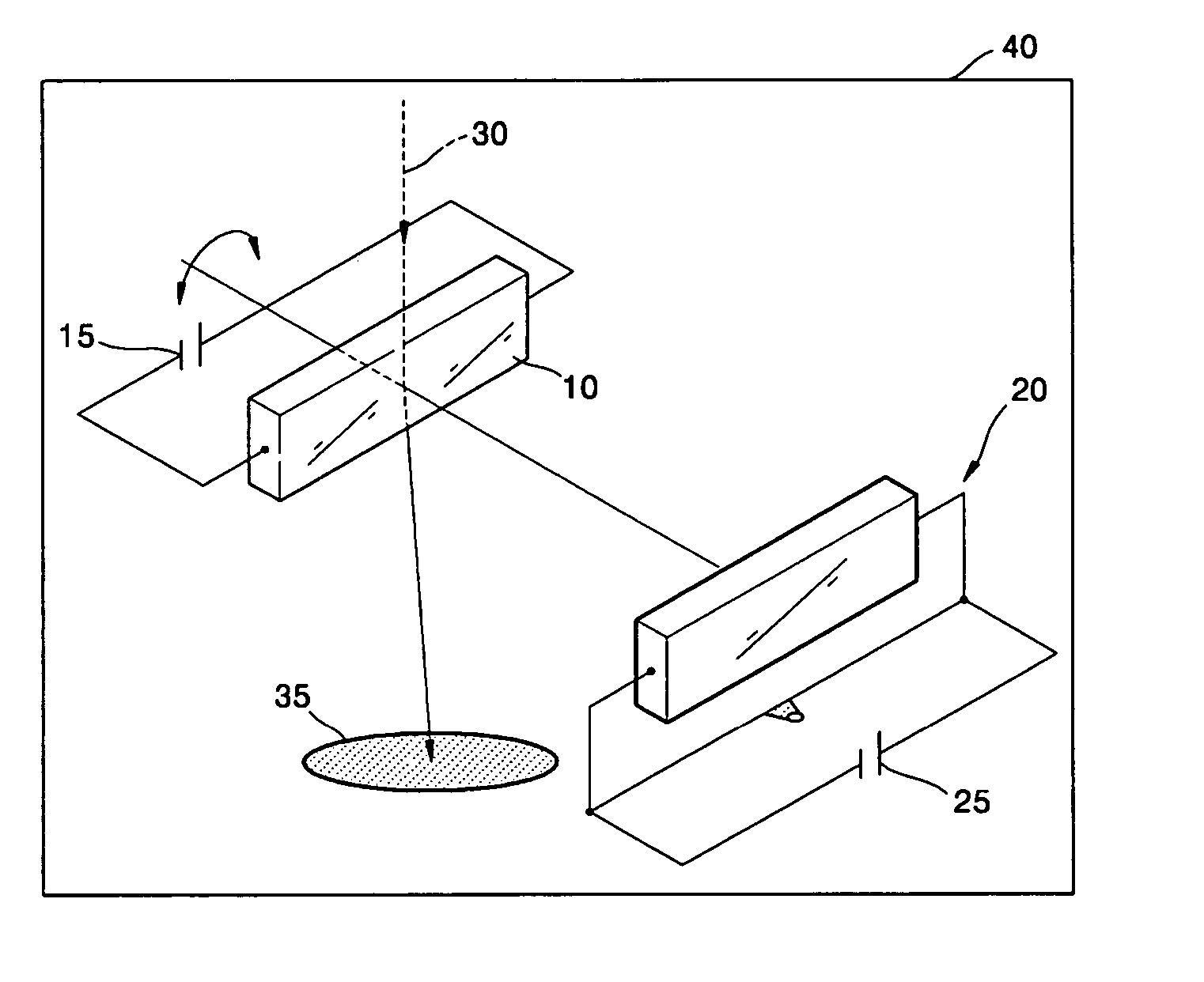
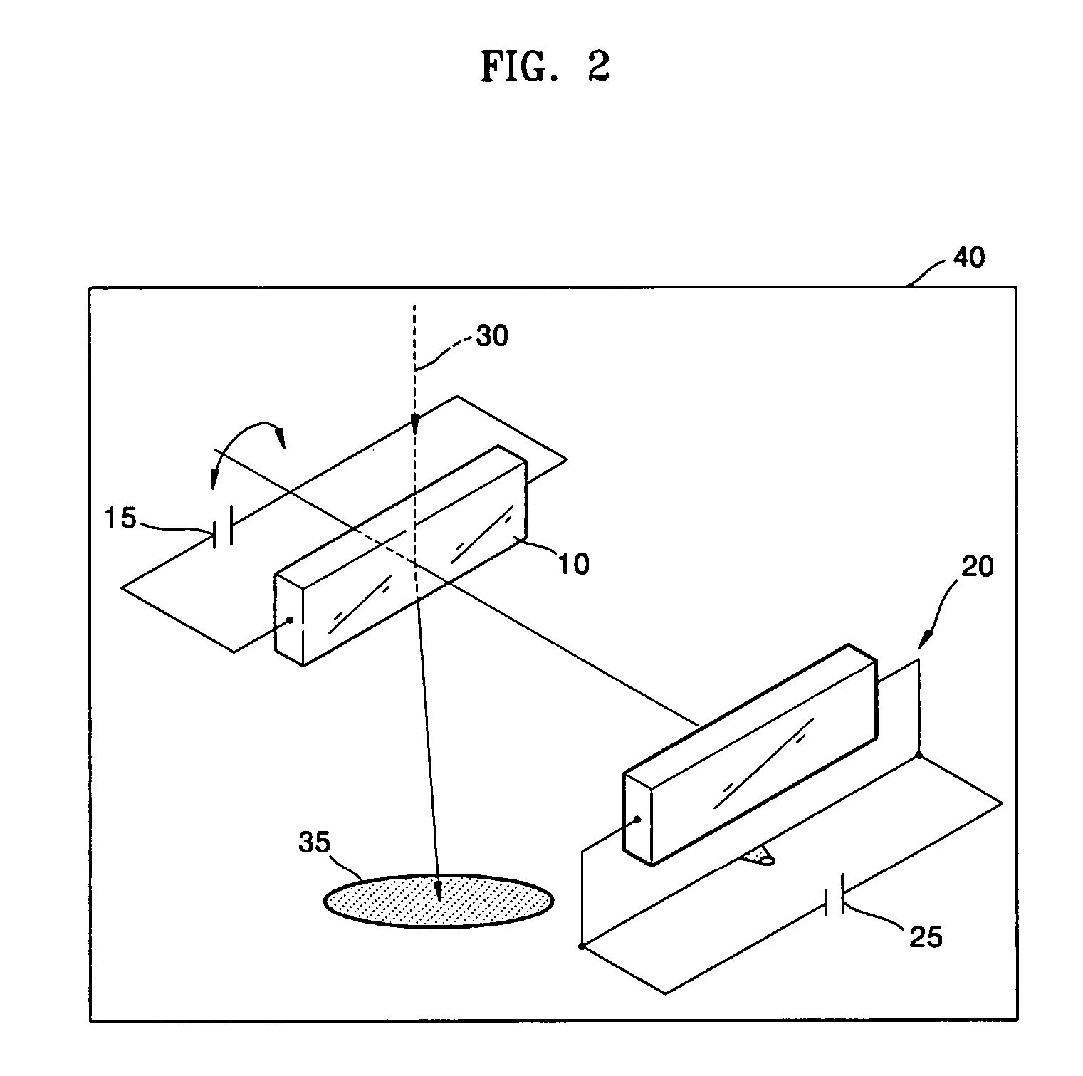
[0022]FIG. 2 schematically illustrates an apparatus for controlling the crystal surface morphology according to the present invention. As illustrated in FIG. 2, the control of the crystal surface morphology according to an embodiment of the present invention may be achieved, for example, in an ultravacuum chamber 40 of an ultra high vacuum reflection electron microscope (UHV-REM). In the ultravacuum chamber 40, a sample crystal substrate 10 and a DC power source 15 for applying a voltage to the sample crystal substrate 10 may be installed. A metal depositing device 20 for depositing metal atoms on the sample crystal substrate 10 and a heater power source 25 for applying a voltage to the metal depositing device 20 may also be installed. Although it is not shown in FIG. 2, a hot plate fo...


PUM

PropertyMeasurementUnit
Temperatureaaaaaaaaaa
Timeaaaaaaaaaa
Pressureaaaaaaaaaa

Abstract

Embodiments include a method of forming a crystal surface with uniform monoatomic steps using metal adsorption. The method of controlling crystal surface morphology may include heating crystal to a predetermined temperature by applying a direct current (DC) voltage to its both ends; and depositing metal atoms to the crystal surface heated to a predetermined temperature at a predetermined depositing rate while maintaining the application of DC voltage so as to form monoatomic steps on the crystal surface.

Description

BACKGROUND OF THE DISCLOSURE [0001] This application claims the benefit of Korean Patent Application No. 10-2004-0063509, filed on Aug. 12, 2004, in the Korean Intellectual Property Office, the disclosure of which is incorporated herein in its entirety by reference. [0002] 1. Field of the Disclosure [0003] Embodiments of the present invention relates to a method of controlling crystal surface morphology using metal adsorption, and more particularly, to a method of forming a crystal surface having uniform monoatomic steps using metal adsorption. [0004] 2. Description of the Related Art [0005] As the importance of nanotechnology is gradually increased, considerable amounts of research on surface reactions and a structure of a crystal at an atomic level are being conducted. In particular, a technology to both form and control a well-defined and stable crystal surface morphology at an atomic level is being investigated. However, there is no attempt to control the crystal surface morphol...

Claims


Application Information

Patent Timeline
IPC IPC(8): H01J37/08
CPCC23C14/16C30B33/04C23C14/26H01L21/20
Inventor SONG, SE-AHNLATYSHEV, ALEXANDER V.KOSOLOBOV, SERGEY S.GUTAKOVSKII, ANTON K.FEDINA, LUDMILA I.
Owner SAMSUNG ELECTRONICS CO LTD
Why Eureka
Try Eureka