Single-crystal substrate,single-crystal substrate having crystalline film,crystalline film,method for producing single-crystal substrate having crystalline film,method for producing crystalline substrate,and method for producing element

a technology of single crystallinity and substrate, which is applied in the direction of instruments, record information storage, transportation and packaging, etc., can solve the problems of cracks between the substrate for growth and the crystalline film, the substrate is difficult to obtain, and the substrate is difficult to grow. , to achieve the effect of inferior crystallinity, inferior crystallinity, and inferior crystallinity

Inactive Publication Date: 2015-08-11
NAMIKI PRECISION JEWEL CO LTD
View PDF19 Cites 0 Cited by
  • Summary
  • Abstract
  • Description
  • Claims
  • Application Information

AI Technical Summary

Benefits of technology

[0068]As described above, according to the present invention, the single-crystal substrate for epitaxial growth on which a crystalline film may be formed with stress thereon being suppressed or eliminated, the single-crystal substrate having a crystalline film, the crystalline film, the method of producing a single-crystal substrate having a crystalline film, the method of producing a crystalline substrate, and the element producing method may be provided.
[0069]Note that, according to the inventions as described in claims 1, 4, 9, 10, 16, 19, and 34, the roughened-surface formed surface and the roughened-surface unformed surface are provided on the surface of the single-crystal substrate for epitaxial growth. This enables, for example, provision of a single-crystalline film portion and a crystalline film portion having inferior crystallinity to the single-crystalline film as the crystalline film to be formed. In this case, by partly providing as the crystalline film the crystalline film having inferior crystallinity to the single-crystalline film, internal stress caused in the entire crystalline film due to a difference in lattice constant and a difference in thermal expansion value with the single-crystal substrate may be relieved to the outside of the crystalline film from the crystalline film portion having inferior crystallinity to the single-crystalline film.
[0070]By relieving the internal stress to the outside of the crystalline film, the amount of warpage of the crystalline film is reduced or eliminated to improve the uniformity of the photolithography step when the respective elements are produced and to prevent development of a crack in the crystalline film. Further, according to the inventions as described in claims 5, 6, 20, and 21, the amount of warpage is reduced or eliminated, and thus, a crystalline film may be formed using a large-diameter substrate of 2 inches or more as the single-crystal substrate. Therefore, a large-diameter crystalline film of 2 inches or more may be formed in one film forming step, and thus, the mass productivity may be improved.
[0071]Further, according to the inventions as described in claims 2 and 17, by forming the pattern of a roughened-surface formed portion on the surface of the single-crystal substrate to be point-symmetric with respect to the center point of the single-crystal substrate, the internal stress may be relieved uniformly over the entire surface of the crystalline film. Further, by causing the pattern to be in the shape of stripes, in the shape of a coil, or symmetric with respect to a line, it is also possible to two-dimensionally and imbalancedly relieve the internal stress of the crystalline film.
[0072]Further, according to the inventions as described in claims 3 and 18, by forming as the pattern the roughened-surface formed portion so as to be partly intermittent to be discontinuous in a plane direction of the single-crystal substrate, when the single-crystal substrate having a crystalline film including the single-crystal substrate and the crystalline film is cut after the crystalline film is formed, the cutting may be carried out so as to obtain a straight cut off line without crossing the roughened-surface formed portion. Therefore, the division step of the single-crystal substrate having a crystalline film may be simplified, and at the same time, a single-crystalline film portion having a large area may be cut out from the crystalline film.
[0073]Further, according to the inventions as described in claims 7 and 32, by setting the width of the roughened surface to be more than 0 μm and 80 μm or less, the area occupied by the roughened surface portion on the surface of the single-crystal substrate may be reduced to inhibit reduction in the number of made elements such as light-emitting elements, photovoltaic elements, or semiconductor elements, and at the same time, after the element portion is manufactured and when the single-crystal substrate is divided into chips of elements, the roughened surface may be used as a division line. Further, according to the inventions as described in claims 8 and 33, by setting the width of the roughened surface to be more than 0 μm and 10 μm or less, the area occupied by the roughened surface portion on the surface of the single-crystal substrate may be further reduced, and thus, the area occupied by the roughened surface portion on the surface of the single-crystal substrate may be further reduced to increase the number of made elements.

Problems solved by technology

However, in order to make a substrate for growth having warpage which cancels warpage caused in the epitaxial growth, that is, having warpage in a direction opposite to that of the warpage caused in the epitaxial growth, by carrying out heat treatment in advance at a temperature that is lower than the temperature at which the warpage is completely relaxed according to the method disclosed in Patent Literature 1, it is necessary to measure the distortion of the substrate for growth prior to the heat treatment and to change the temperature of the heat treatment according to the amount of the distortion, which is not suitable for mass production and results in increase in cost of the substrate.
In addition, the temperature in the epitaxial growth is ordinarily higher than the temperature of the heat treatment and distortion intentionally caused to remain is relaxed during the epitaxial growth, and thus, it is extremely difficult to obtain the substrate for growth and the crystalline film having the target amount of warpage after the epitaxial growth, and warpage remains in the substrate for growth and the crystalline film after the epitaxial growth.
Therefore, when an attempt is made to affix the substrate for growth to a lapping machine for lapping treatment of a rear surface of the substrate for growth, the substrate for growth and the crystalline film are required to be pressed with heavy pressure against the lapping machine due to the warpage, and the pressure causes a crack in the substrate for growth and the crystalline film.
However, the size of the nitride semiconductor film is too small, and thus, taking mass productivity into consideration, formation of a relatively large-sized nitride semiconductor film of, for example, 2 inches or more is desired.

Method used


Image

  • Single-crystal substrate,single-crystal substrate having crystalline film,crystalline film,method for producing single-crystal substrate having crystalline film,method for producing crystalline substrate,and method for producing element
  • Single-crystal substrate,single-crystal substrate having crystalline film,crystalline film,method for producing single-crystal substrate having crystalline film,method for producing crystalline substrate,and method for producing element
  • Single-crystal substrate,single-crystal substrate having crystalline film,crystalline film,method for producing single-crystal substrate having crystalline film,method for producing crystalline substrate,and method for producing element

Examples


examples

[0163]Next, examples of the present invention are described, but the present invention is not limited to the following examples.

examples 1 to 4

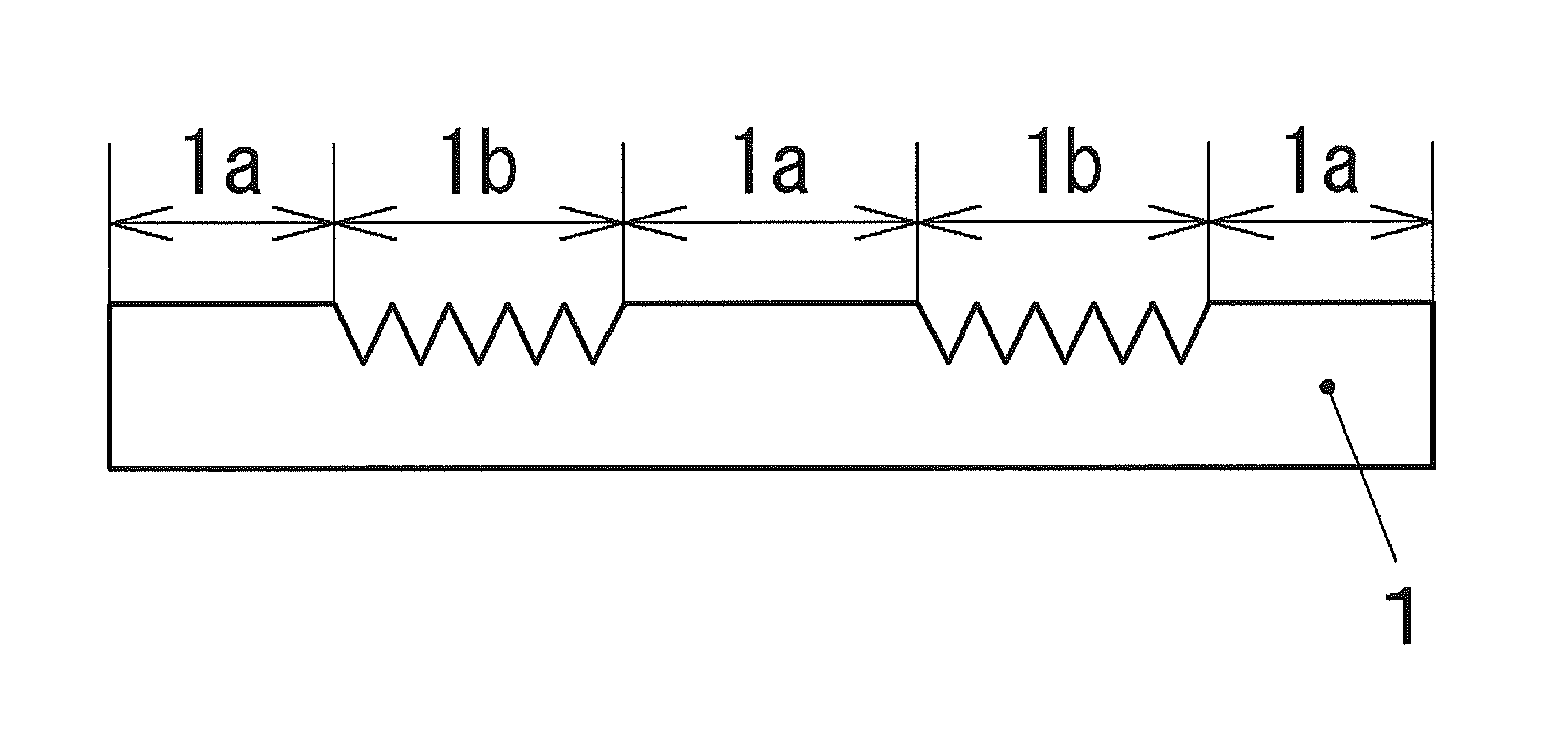
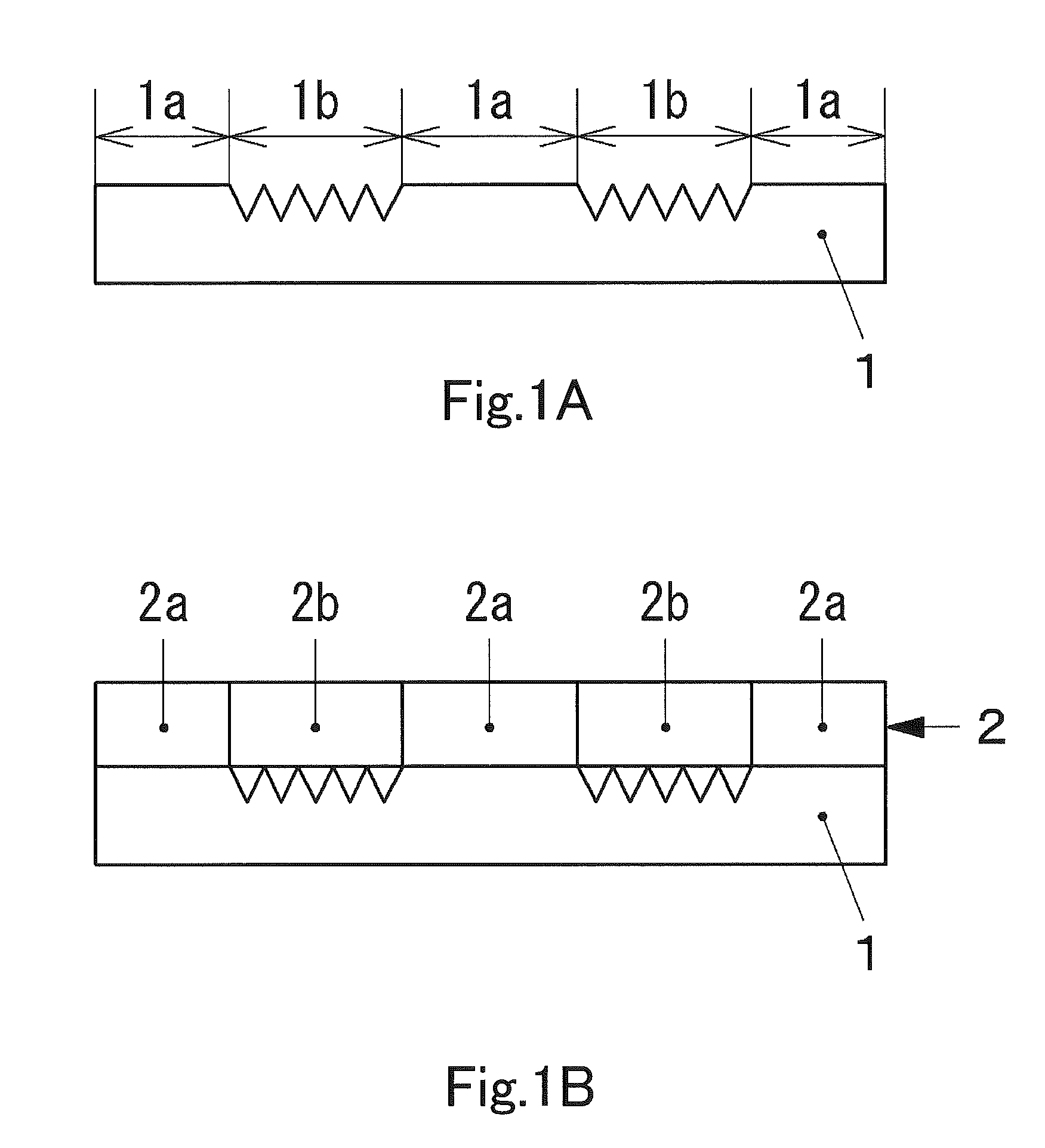
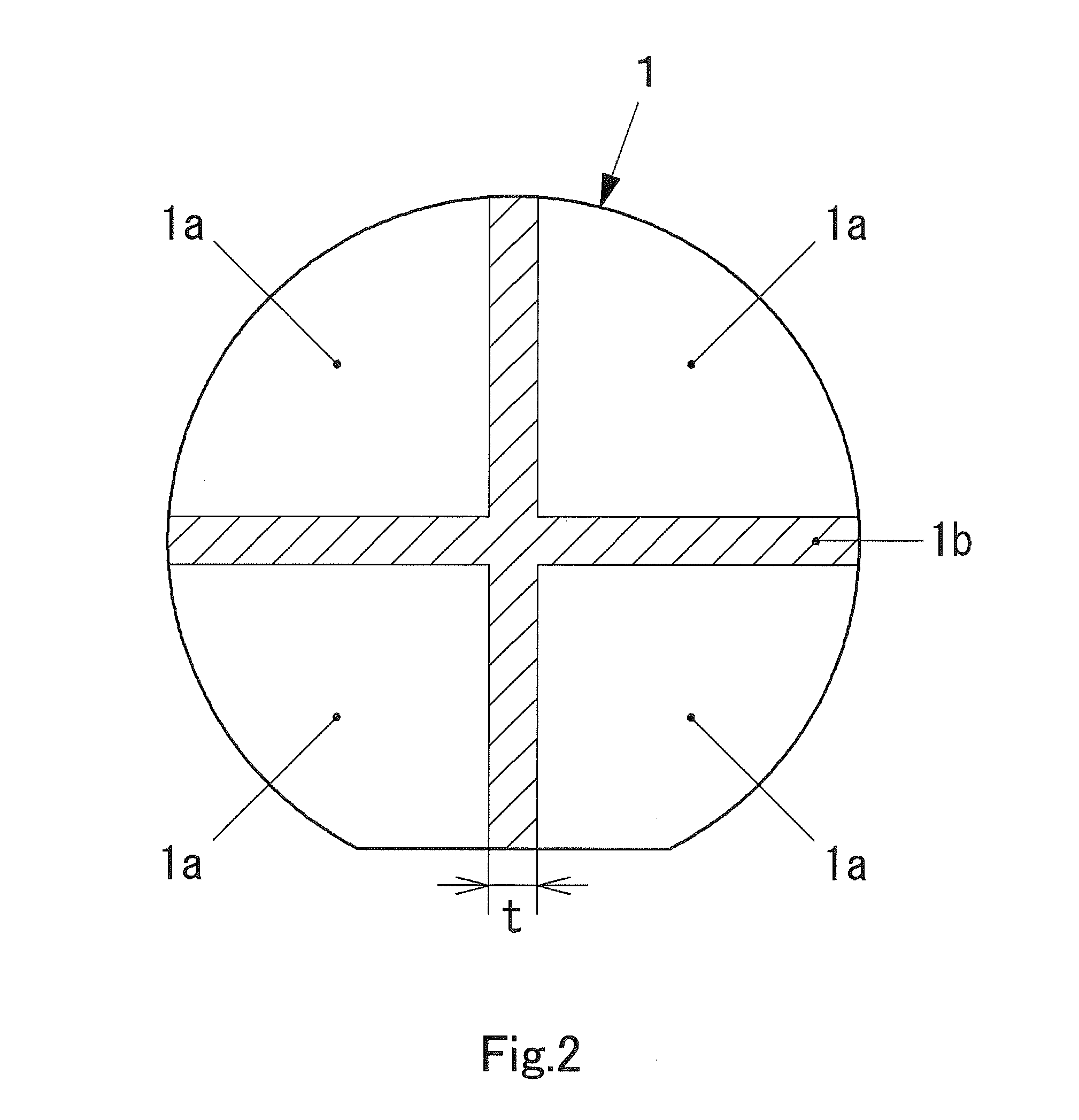
[0164]As Examples 1 to 4, the curvature behavior of the single-crystal substrate 1 is described when the buffer layer was formed and the crystalline film 2 formed by laminating the n-GaN-based layer and the InGaN-based active layer was epitaxially grown on the single-crystal substrate 1, in which the pattern of the roughened surface 1b was set to be in the shape of a cross formed so as to be perpendicular to and in parallel to the orientation flat surface of the single-crystal substrate 1 as illustrated in FIG. 2.

[0165]As samples for evaluation, the single-crystal substrate 1 having the crystalline film 2 was made, in which the buffer layer and the crystalline film 2 including the n-GaN-based layer and the InGaN-based active layer were formed on the one surface of the single-crystal substrate 1 corresponding to the crystal growth surface, the single-crystal substrate 1 having the shape of the pattern of the roughened surface illustrated in FIG. 2 and being made of sapphire. The curv...

examples 5 to 7

[0184]As Examples 5 to 7, the curvature behavior of the single-crystal substrate 1 is described below when the buffer layer was formed and the crystalline film 2 formed by laminating the n-GaN-based layer and the InGaN-based active layer was epitaxially grown on the single-crystal substrate 1, in which the pattern of the roughened surface 1b was set to be in the shape of a cross formed so as to be perpendicular to and in parallel to the orientation flat surface of the single-crystal substrate 1 as illustrated in FIG. 3.

[0185]As samples for evaluation, the single-crystal substrate 1 having the crystalline film 2 was made, in which the buffer layer and the crystalline film 2 including the n-GaN-based layer and the InGaN-based active layer were formed on the one surface of the single-crystal substrate 1 corresponding to the crystal growth surface, the single-crystal substrate 1 having the shape of the pattern of the roughened surface illustrated in FIG. 3 and being made of sapphire. Th...


PUM

PropertyMeasurementUnit
diameteraaaaaaaaaa
widthaaaaaaaaaa
widthaaaaaaaaaa

Abstract

Provided are a single-crystal substrate for epitaxial growth on which a crystalline film may be formed with stress thereon being suppressed or eliminated, a single-crystal substrate having a crystalline film, a crystalline film, a method of producing a single-crystal substrate having a crystalline film, a method of producing a crystalline substrate, and an element producing method. The single-crystal substrate has a roughened surface formed on at least a partial region of a surface of the single-crystal substrate. And in order to obtain the single-crystal substrate having a crystalline film, a single-crystalline film is formed by epitaxial growth on a roughened-surface unformed surface on which the roughened surface is not formed, and a crystalline film having low crystallinity than the single-crystalline film is formed by epitaxial growth on a roughened-surface formed surface of the single-crystal substrate.

Description

CROSS REFERENCE TO RELATED APPLICATIONS[0001]This is a U.S. national stage of application No. PCT / JP2011 / 058734, filed on 6 Apr. 2011. Priority under 35 U.S.C. §119 (a) and 35 U.S.C. §365 (b) is claimed from Japanese Application Nos. 2010-092614, filed 13 Apr. 2011 and JP 2010-148880, filed 30 Jun. 2010, the disclosure of which are also incorporated herein by reference.TECHNICAL FIELD[0002]The present invention relates to a single-crystal substrate, a single-crystal substrate having a crystalline film, a crystalline film, a method of producing a single-crystal substrate having a crystalline film, a method of producing a crystalline substrate, and an element producing method.BACKGROUND ART[0003]A nitride semiconductor represented by gallium nitride (GaN) has a wide band gap and is capable of emitting blue light, and thus, is widely used for a light-emitting diode (LED), a semiconductor laser (LD), and the like. For example, a white LED in which a blue LED containing GaN and a substan...

Claims


Application Information

Patent Timeline
Patent Type & Authority Patents(United States)
IPC IPC(8): B32B3/00C30B29/40C30B25/18H01L21/02
CPCC30B25/18C30B29/403H01L21/0242H01L21/0243H01L21/0254H01L21/02658Y10T428/21Y10T428/24355
Inventor AIDA, HIDEOAOTA, NATSUKO
Owner NAMIKI PRECISION JEWEL CO LTD
Why Eureka
Try Eureka