Semiconductor device manufacturing apparatus and a method of controlling a semiconductor device manufacturing process

a manufacturing apparatus and semiconductor technology, applied in the direction of discharge tube/lamp details, nuclear engineering, testing/measurement of semiconductor/solid-state devices, etc., can solve the problems of inability to be practicable in many instances, process can be affected in a harmful way, etc., to minimise the effect of reducing the production of contaminant particles

Inactive Publication Date: 2006-02-16
APPLIED MATERIALS INC
View PDF11 Cites 4 Cited by
  • Summary
  • Abstract
  • Description
  • Claims
  • Application Information

AI Technical Summary

Benefits of technology

[0026] In this way, a measure of contaminant particle flux is used to adjust a process parameter with a view to minimising the production of contaminant particles in the process.
[0027] Preferably, the method described above is applied during an initial setting up or calibration procedure, before process wafers are exposed to the desired process conditions in the vacuum chamber. In this way, the process parameters themselves can be adjusted with a view to minimising the production of contaminant particles in the process.
[0028] For example, in an ion beam implantation process, process parameters controlling the ion beam itself may be adjusted in accordance with the above described method, to minimise particle production. The adjusted process parameters may include those controlling the lateral alignment of the beam through the beam line, or parameters controlling the voltage on electrostatic focussing elements of the beam line. The method of the invention for the first time permits these parameters to be optimised for low particle production, and the optimisation may be performed dynamically, in the sense that the effect of parameter change on measured particle flux can be monitored to confirm reduction
[0029] As mentioned above, the optimisation or controlling process may be conducted as a preliminary set up procedure, but also may be conducted during a live process run to adjust parameters which are not process-critical in order to minimise particle production.
[0030] Importantly, the method described above is conducted whilst process conditions are maintained within the vacuum chamber, so that the effect of the controlling method is to provide a closed loop enabling the effect of parameter adjustments in reducing contaminant particle flux to be monitored.

Problems solved by technology

It is well understood that the processes can be affected in a harmful way by the presence on the surface of the substrate or wafer being processed of contaminant particulates which may be derived from within the process chamber.
Although in some cases it might then be possible to restart the process with the previously part processed wafers, in order to complete the processing of those wafers, this may not be practicable in many instances.
Exceeding the higher threshold value may be the result of a so called catastrophic event, such as a wafer breakage within the chamber.

Method used


Image

  • Semiconductor device manufacturing apparatus and a method of controlling a semiconductor device manufacturing process
  • Semiconductor device manufacturing apparatus and a method of controlling a semiconductor device manufacturing process
  • Semiconductor device manufacturing apparatus and a method of controlling a semiconductor device manufacturing process

Examples


Embodiment Construction

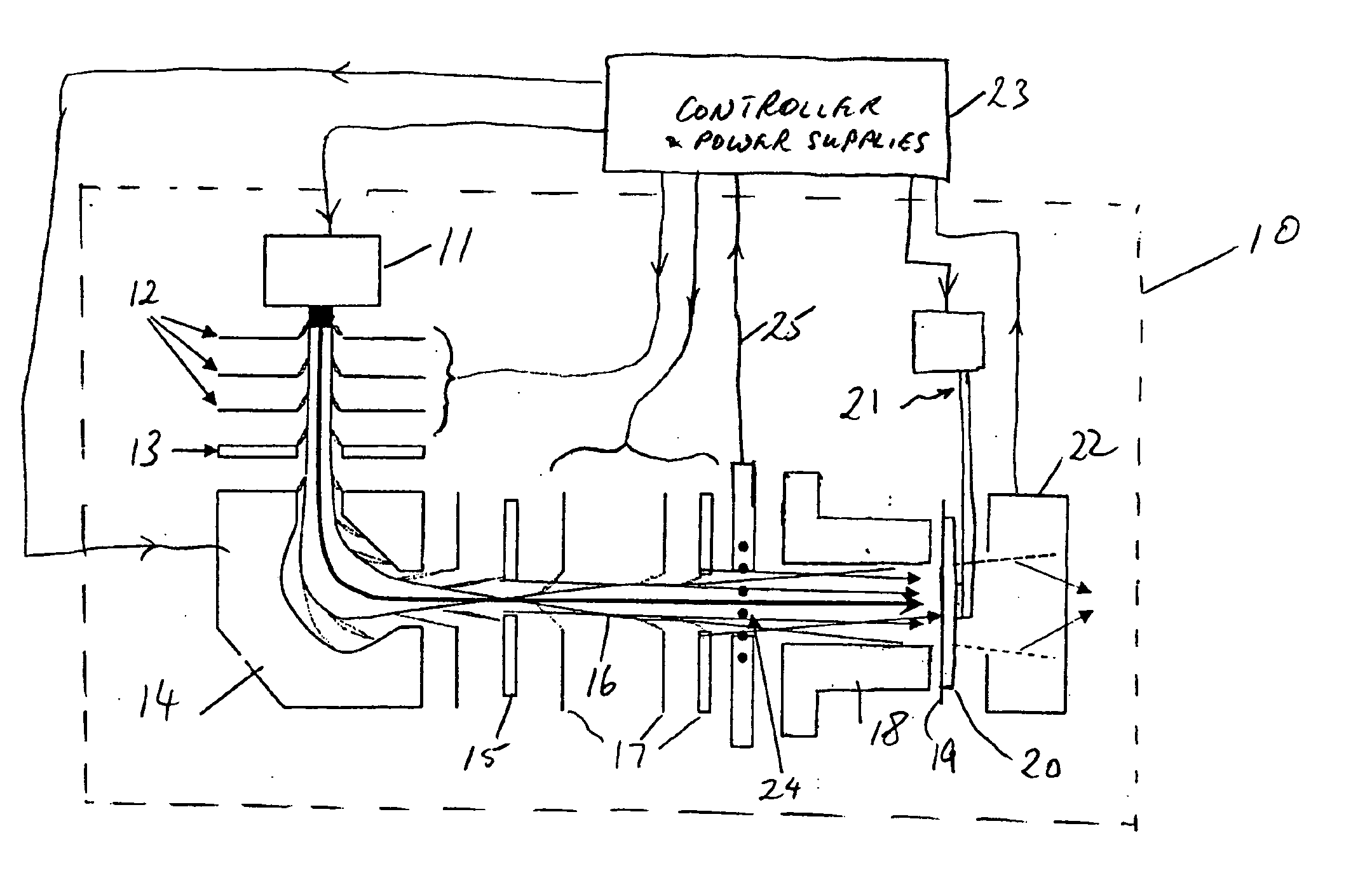
[0039] Referring to FIG. 1, the main parts of a typical ion implanter are illustrated within a vacuum chamber illustrated schematically by the box 10. Ions are generated in an ion source 11, e.g. a Bernas type ion source, and extracted to form a beam by extraction electrodes 12. The beam of extracted ions passes through an aperture in shielding or baffle 13 to enter the flight tube of analyser magnet 14. Within the analyser magnet 14, ions in the beam having different mass-to-charge ratios adopt different flight path curvatures and so becomes spatially separated at the exit of the analyser. A mass resolution slit 15 is located at the exit of the analyser to select ions of a desired mass-to-charge ratio for onward transmission and implantation.

[0040] In this embodiment, a beam 16 of mass selected ions passes through focussing lenses 17, which may for example be used for accelerating or decelerating the beam to a desired implant energy. The focussed beam passes through a plasma flood...


PUM

PropertyMeasurementUnit
mass-to charge ratioaaaaaaaaaa
energyaaaaaaaaaa
bias potentialaaaaaaaaaa

Abstract

A particle monitor in the process chamber of a semiconductor device manufacturing apparatus provides a measure of a flux of contaminant particles in the chamber. The flux is measured whilst process conditions are produced in the process chamber and a process parameter is adjusted in response to the measured flux in order to reduce this flux during the process. In an ion implanter, the particle sensor measures the flux of particles entrained with the ion beam at a location in front of the wafer being processed.

Description

FIELD OF THE INVENTION [0001] This invention relates to the control of processes for manufacturing semiconductor devices in which desired process conditions are provided in a vacuum chamber. The invention is also concerned with improvements in semiconductor device manufacturing apparatus. BACKGROUND OF THE INVENTION [0002] Semiconductor manufacturing processes are used for creating and modifying structures in substrates of semiconductor material in order to create useful devices in the substrate. Many of these manufacturing processes are conducted on substrates or wafers of the semiconductor material held in a vacuum chamber and exposed to the desired process conditions. It is well understood that the processes can be affected in a harmful way by the presence on the surface of the substrate or wafer being processed of contaminant particulates which may be derived from within the process chamber. Unwanted particulates within the process chamber can be derived from a number of sources...

Claims


Application Information

Patent Timeline
Patent Type & Authority Applications(United States)
IPC IPC(8): H01L21/66H01J7/24H01L21/425B05C11/00C23C14/56H01J37/317
CPCC23C14/564H01J2237/0225H01J37/3171H01L21/265
Inventor SIMMONS, JONATHON YANCEY
Owner APPLIED MATERIALS INC
Why Eureka
Try Eureka