Fabrication method of light emitting diode incorporating substrate surface treatment by laser and light emitting diode fabricated thereby

a technology of light emitting diodes and fabrication methods, which is applied in the manufacture of semiconductor/solid-state devices, electrical devices, semiconductor devices, etc., can solve the problems of low light extraction efficiency, difficulty in realizing fine geometry, and light loss, and achieve the effect of improving the light extraction efficiency of leds

Inactive Publication Date: 2006-02-23
SAMSUNG ELECTRONICS CO LTD
View PDF5 Cites 82 Cited by
  • Summary
  • Abstract
  • Description
  • Claims
  • Application Information

AI Technical Summary

Benefits of technology

[0017] The present invention has been made to solve the foregoing problems of the prior art and it is therefore an object of the present invention to provide a fabrication method of LEDs incorporating a step of surface-treating a substrate by a laser to implement fin...

Problems solved by technology

However, such a flip-chip LED 10 has following problems.
This as a result causes light loss thereby to lower the light extraction efficiency and thus the external quantum efficiency of the flip-chip LED 10.
However, these approaches produce a roughened structure in common through chemical etching and thus disadvantageously have a difficulty in realizing a fine geometry.
Since a substrate for example of sapphire is resistant to etching, harsh etching conditions are necessary.
As a result, those etching techniques using photoresists can hardly form fine surface geometries for example of pore or pillar size under 1 μm in substrates.
Of course, it is muc...

Method used


Image

  • Fabrication method of light emitting diode incorporating substrate surface treatment by laser and light emitting diode fabricated thereby
  • Fabrication method of light emitting diode incorporating substrate surface treatment by laser and light emitting diode fabricated thereby
  • Fabrication method of light emitting diode incorporating substrate surface treatment by laser and light emitting diode fabricated thereby

Examples


first embodiment

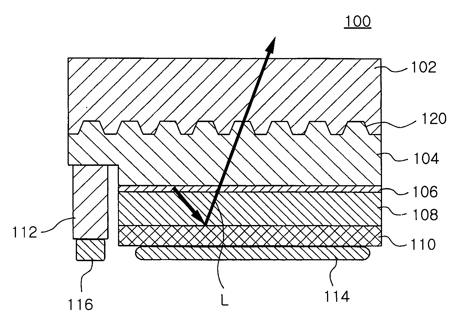
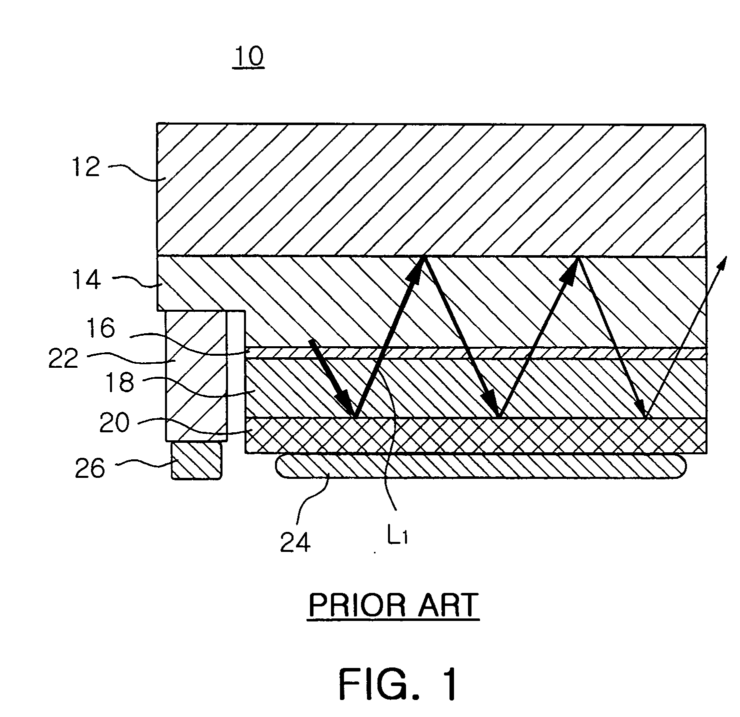
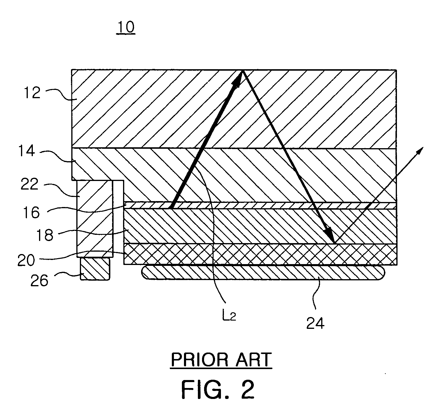
[0043]FIG. 3 is a flowchart of an LED fabrication method according to the present invention. Referring to FIG. 3, a substrate of for example sapphire is prepared in S102, and a laser beam is emitted onto one side of the sapphire substrate to form a fine roughened structure in S104. Then, semiconductor layers including an n-GaN layer, an active layer and a p-GaN layer are formed in succession on the roughened surface of the sapphire substrate in S106, S108 and S110, and a resultant structure is etched into a mesa structure in S112. Then, a p-electrode is formed on the p-GaN layer and an n-electrode is formed on an exposed partial area of the n-GaN layer to complete an LED in S114.

[0044] In order to form a fine roughened structure in the substrate surface, the present invention can utilize various lasers including 308 nm, 428 nm and 198 nm Excimer lasers, an Nd:YAG laser (YAG is the short form of Yttrium Aluminum Garnet), a He—Ne laser and an Ar-ion laser. These lasers can easily form...

second embodiment

[0050]FIG. 5 is a flowchart of an LED fabrication method according to the present invention. Referring to FIG. 5, a substrate of for example sapphire is prepared in S202, one side of the sapphire substrate is pre-treated in S204, a plurality of semiconductor layers including n-GaN, active and p-GaN layers are formed in their order on the treated side of the sapphire substrate in S206, S208 and S210, and a resultant structure is mesa-etched to expose a partial area of the n-GaN layer in S212. A p-electrode is formed on the p-GaN layer and an n-GaN layer is formed on the exposed area of the n-GaN layer in S214. Then, the sapphire substrate is polished at the other side with a grinder containing for example diamond slurry to reduce the thickness of the sapphire substrate and then a laser beam is illuminated onto the other side of the sapphire substrate to form a fine roughened structure in S216.

[0051] In order to form a fine roughened structure in the substrate surface, this embodiment...

third embodiment

[0056]FIG. 7 is a flowchart of an LED fabrication method according to the present invention. Referring to FIG. 7, a substrate of for example sapphire is prepared in S302, a laser beam is emitted onto one side of the sapphire substrate to form a fine roughened structure in S304, an n-GaN layer, an active layer and a p-GaN layer are formed in their order on the roughened side of the sapphire substrate in S306, S308 and S310, and a resultant structure is mesa-etched to expose a partial area of the n-GaN layer in S312. A p-electrode is formed on the p-GaN layer and an n-electrode is formed on the exposed area of the n-GaN layer in S314. Then, the sapphire substrate is polished at the other side with a grinder containing for example diamond slurry to reduce the thickness of the sapphire substrate and then a laser beam is emitted onto the other side of the sapphire substrate to form a fine roughened structure in S316.

[0057] In this embodiment, the process steps of forming the fine roughen...


PUM


Abstract

The present invention relates to a fabrication method of LEDs incorporating a step of surface-treating a substrate by a laser and an LED fabricated by such a fabrication method. The present invention can use a laser in order to implement finer surface treatment to an LED substrate over the prior art. As a result, the invention can improve the light extraction efficiency of an LED while protecting the substrate from chronic problems of the prior art such as stress or defects induced from chemical etching and/or physical polishing.

Description

RELATED APPLICATION [0001] The present application is based on, and claims priority from, Korean Application Number 2004-64535, filed Aug. 17, 2004, the disclosure of which is hereby incorporated by reference herein in its entirety. BACKGROUND OF THE INVENTION [0002] 1. Field of the Invention [0003] The present invention relates to a Light Emitting Diode (LED), and in particular, to a fabrication method of LEDs incorporating a step of surface-treating a substrate by a laser and an LED fabricated by such a fabrication method. More particularly, the present invention can use a laser in order to implement finer surface treatment to an LED substrate over the prior art thereby improving the light extraction efficiency of an LED while protecting the substrate from chronic problems of the prior art such as stress or defects induced from chemical etching and / or physical polishing. [0004] 2. Description of the Related Art [0005] In general, nitride semiconductors such as InAlGaN are widely u...

Claims


Application Information

Patent Timeline
IPC IPC(8): H01L33/00H01L33/22
CPCH01L33/007H01L33/22H01L21/02378H01L21/02403Y10S438/964H01L21/0243H01L21/02458H01L21/0254H01L21/0242
Inventor PARK, YOUNG HOHAHM, HUN JOOKO, KUN YOOCHO, HYO KYOUNG
Owner SAMSUNG ELECTRONICS CO LTD
Why Eureka
Try Eureka