Electrode structure of a semiconductor device and method of manufacturing the same

a semiconductor device and electromechanical technology, applied in the direction of printed circuit, sustainable manufacturing/processing, final product manufacturing, etc., can solve the problems of increasing ic chip processing speed and ic chip pin count, interconnection becomes impaired, and new improved technology for fine-pitch wire bonding structures cannot keep pace with demand

Inactive Publication Date: 2006-02-23
SAMSUNG ELECTRONICS CO LTD
View PDF9 Cites 181 Cited by
  • Summary
  • Abstract
  • Description
  • Claims
  • Application Information

AI Technical Summary

Problems solved by technology

New improved technologies for achieving fine-pitch wire bonding structures cannot keep pace with the demand resulting from increased IC chip processing speeds and higher IC chip pin counts.
The larger the cracks, the more the interconnection becomes impaired, and device failures can readily occur when cracks propagate completely through the solder bump structure.
In practice,

Method used


Image

  • Electrode structure of a semiconductor device and method of manufacturing the same
  • Electrode structure of a semiconductor device and method of manufacturing the same
  • Electrode structure of a semiconductor device and method of manufacturing the same

Examples


Embodiment Construction

[0027] The present invention will now be described in detail with reference to preferred, but non-limiting, embodiments of the invention.

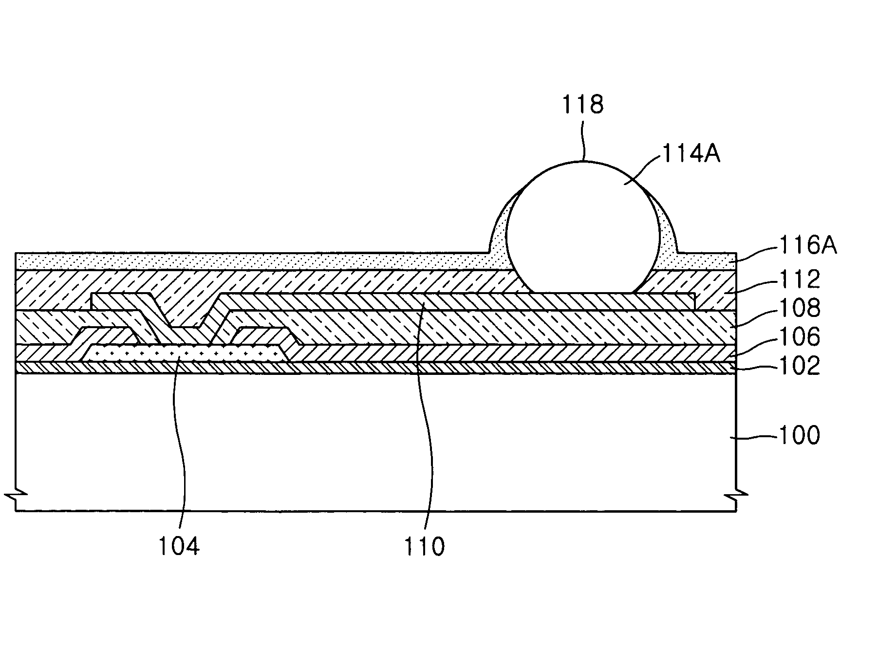
[0028]FIGS. 4A through 4G are schematic cross-sectional views for explaining a method of manufacturing a semiconductor package according to an embodiment of the present invention.

[0029] Referring initially to FIG. 4A, a semiconductor structure is fabricated or provided so as to generally include a semiconductor substrate 100, an integrated circuit layer 102, a chip pad 104, a passivation layer 106, and an insulating layer 108. The insulating layer may, for example, be formed of BCB (Benzo Cyclo Butene), polyimide, epoxy, silicon oxide, silicon nitrite, or composites of these materials. Also, as shown, an opening is formed through the passivation layer 106 and the insulating layer 108 to expose a top surface region of the chip pad 104. In this example, the insulating layer 108 extends to the surface of the chip pad 104, and accordingly, the sidewa...


PUM

PropertyMeasurementUnit
Temperatureaaaaaaaaaa
Angleaaaaaaaaaa
Angleaaaaaaaaaa

Abstract

In the manufacture of a semiconductor device, a photosensitive layer is deposited to cover an exposed portion of an electrode with the photosensitive layer. The photosensitive layer is then subjected to a photolithography process to partially remove the photosensitive layer covering the electrode. The electrode may be a ball electrode or a bump electrode, and the semiconductor device may be contained in a wafer level package (WLP) or flip-chip package.

Description

BACKGROUND OF THE INVENTION [0001] 1. Field of the Invention [0002] The present invention generally relates to integrated circuit (IC) chips and packages, and more particularly, the present invention relates to the electrode structures of IC chips and devices, and to methods of forming electrode structures for IC chips and packages. [0003] 2. Description of the Related Art [0004] As integrated circuits (IC's) advance toward higher speeds and larger pin counts, first-level interconnection techniques employing wire bonding technologies have approached or even reached their physical limits. New improved technologies for achieving fine-pitch wire bonding structures cannot keep pace with the demand resulting from increased IC chip processing speeds and higher IC chip pin counts. Accordingly, the current trend is to replace wire bonding structures with other package structures, such as a flip chip packages and wafer level packages (WLP). [0005] Flip chip packages and WLP structures are pa...

Claims


Application Information

Patent Timeline
IPC IPC(8): H01L23/48H01L21/44
CPCH01L21/563Y10T29/49149H01L23/3128H01L23/3171H01L23/525H01L24/11H01L24/12H01L2224/0231H01L2224/13099H01L2224/16H01L2224/73253H01L2924/01013H01L2924/01015H01L2924/01022H01L2924/01029H01L2924/01033H01L2924/01074H01L2924/01079H01L2924/12044H01L2924/14H01L2924/15311H01L2924/16195H05K3/0023H05K3/3436H05K2201/10977H01L2224/05548H01L2224/05567H01L2224/10126H01L2224/13022H01L2924/01006H01L2924/01024H01L2924/014H01L2924/0002H01L23/3114H01L2224/0401H01L2224/11334H01L2224/05552H01L24/05H01L24/13H01L2224/05655Y02P70/50H01L2924/00014H01L2924/013H01L23/12H01L23/28H01L23/485H01L23/50
Inventor CHUNG, HYUN-SOOSIM, SUNG-MINPARK, MYEONG-SOONJANG, DONG-HYEONSONG, YOUNG-HEE
Owner SAMSUNG ELECTRONICS CO LTD
Why Eureka
Try Eureka