

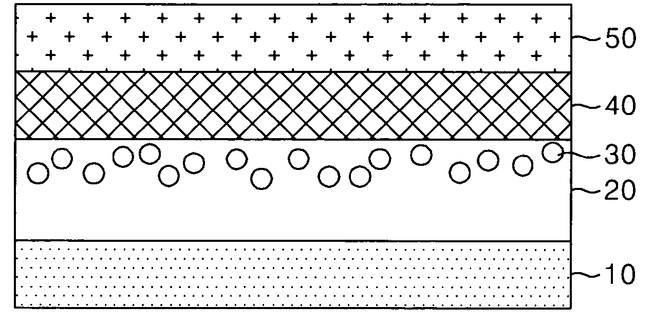
White light-emitting organic-inorganic hybrid electroluminescence device comprising semiconductor nanocrystals
a hybrid electroluminescence and organic technology, applied in the direction of discharge tube luminescnet screens, energy-saving lighting, sustainable buildings, etc., can solve the problems of patents that disclose a white light-emitting organic electroluminescence device, devices that are not driven by electroluminescence,
- Summary
- Abstract
- Description
- Claims
- Application Information
AI Technical Summary
Problems solved by technology
Method used
Image

Examples
example 1
Fabrication of Organic-Inorganic Hybrid Electroluminescence Device Wherein Hole Transport Layer and Nanocrystals Simultaneously Emit Light
[0048] First, a glass substrate on which ITO was patterned was sequentially washed with a neutral detergent, deionized water and isopropyl alcohol, and was then subjected to UV-ozone treatment. poly(9,9′-dioctylfluorene-co-N-(4-butylphenyl)diphenylamine (TFB) and the 520 nm light-emitting CdSe / ZnS nanocrystals prepared in Preparative Example 1 in a weight ratio of 1:1 were dispersed in chlorobenzene to a 1 wt % dispersion. The dispersion was spin-coated on the substrate to a thickness of about 50 nm to form a thin film, and thereafter the thin film was baked at 180° C. for 10 minutes to form a hole transport layer and a semiconductor nanocrystal layer that is light-emitting.
[0049] 3-phenyl-4-(1′-naphthyl)-5-phenyl-1,2,4-triazole (TAZ) was deposited on the completely dried light-emitting layer to form a hole-blocking layer having a thickness of 1...
example 2
Fabrication of Organic-Inorganic Hybrid Electroluminescence Device Wherein Electron Transport Layer and Nanocrystals Simultaneously Emit Light
[0051] First, a glass substrate on which ITO was patterned was sequentially washed with a neutral detergent, deionized water and isopropyl alcohol, and was then subjected to UV-ozone treatment. N,N′-bis(3-methylphenyl)-N,N′-bis(phenyl)benzidine (TPD) and the 470 nm light-emitting nanocrystals prepared in Preparative Example 2 in a weight ratio of 1:1 were dissolved in chloroform to prepare a 1 wt % solution. The solution was spin-coated on the substrate to form a thin film, and thereafter the thin film was baked at 50° C. for 10 minutes to form a hole transport layer and a semiconductor nanocrystal layer that is light-emitting.
[0052] TAZ was deposited on the completely dried light-emitting layer to form a hole-blocking layer having a thickness of 10 nm, and then Alq3 was deposited on the hole-blocking layer to a thickness of about 30 nm to f...
example 3
Fabrication of Organic-Inorganic Hybrid Electroluminescence Device Wherein Different Nanocrystals Simultaneously Emit Light
[0054] First, a glass substrate on which ITO was patterned was sequentially washed with a neutral detergent, deionized water and isopropyl alcohol, and was then subjected to UV-ozone treatment. TPD, the 470 nm light-emitting nanocrystals prepared in Preparative Example 2, and the 590 nm light-emitting nanocrystals prepared in Preparative Example 3 in a weight ratio of 1:0.5:0.5 were dissolved in chloroform to prepare a 1 wt % solution. The solution was spin-coated on the substrate to form a thin film, and thereafter the thin film was baked at 50° C. for 10 minutes to form a hole transport layer and a semiconductor nanocrystal layer that is light-emitting.
[0055] TAZ was deposited on the completely dried light-emitting layer to form a hole-blocking layer having a thickness of 10 nm, and then Alq3 was deposited on the hole-blocking layer to a thickness of about 3...
PUM
 Abstract
Description
Claims
Application Information