Bonding of substrates

a technology of substrates and bonding, which is applied in the manufacture of semiconductor/solid-state devices, semiconductor devices, electrical equipment, etc., can solve the problems of large stresses in between wafers, bonded wafers breaking or delaminating at room temperatur

Inactive Publication Date: 2006-03-02
INTEL CORP
View PDF8 Cites 14 Cited by
  • Summary
  • Abstract
  • Description
  • Claims
  • Application Information

AI Technical Summary

Problems solved by technology

Bonding of these wafers requires an elevated temperature, resulting in large stresses in between wafers upon return to room temperature due to a ...

Method used


Image

  • Bonding of substrates
  • Bonding of substrates
  • Bonding of substrates

Examples


Embodiment Construction

[0012] In the following description, for purposes of explanation, numerous details are set forth in order to provide a thorough understanding of the disclosed embodiments of the present invention. However, it will be apparent to one skilled in the art that these specific details are not required in order to practice the disclosed embodiments of the present invention.

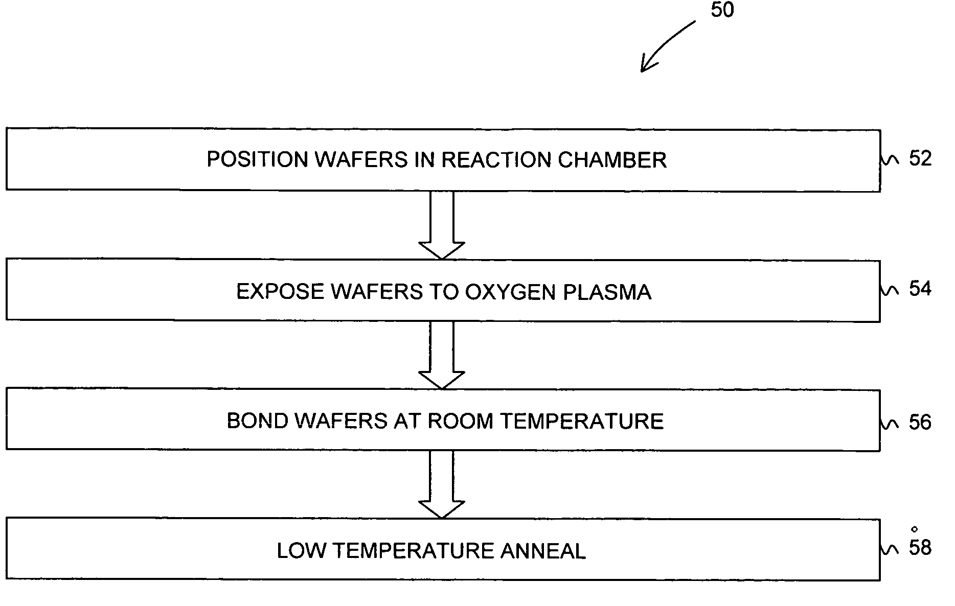
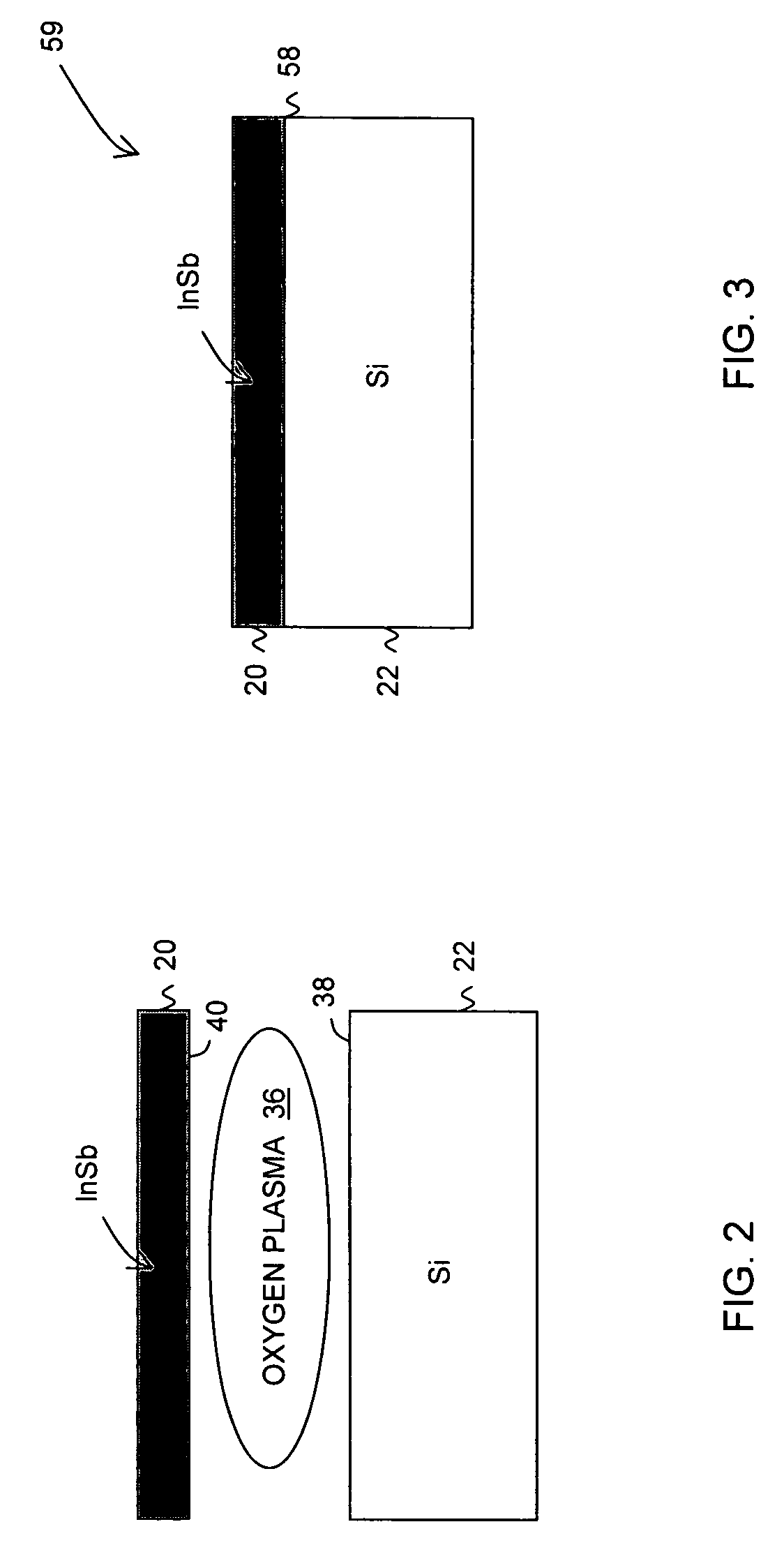
[0013] In one embodiment and method according to the present invention, an indium antimonide (InSb) substrate is directly bond to a silicon (Si) substrate or a silicon dioxide (SiO2) substrate at room temperature after an oxygen plasma surface activation in a reaction chamber. One of many possible plasma surface activation devices that may be used to achieve this direct bonding is first described, followed by a description of the direct bonding process using this plasma surface activation device according to one method of the present invention.

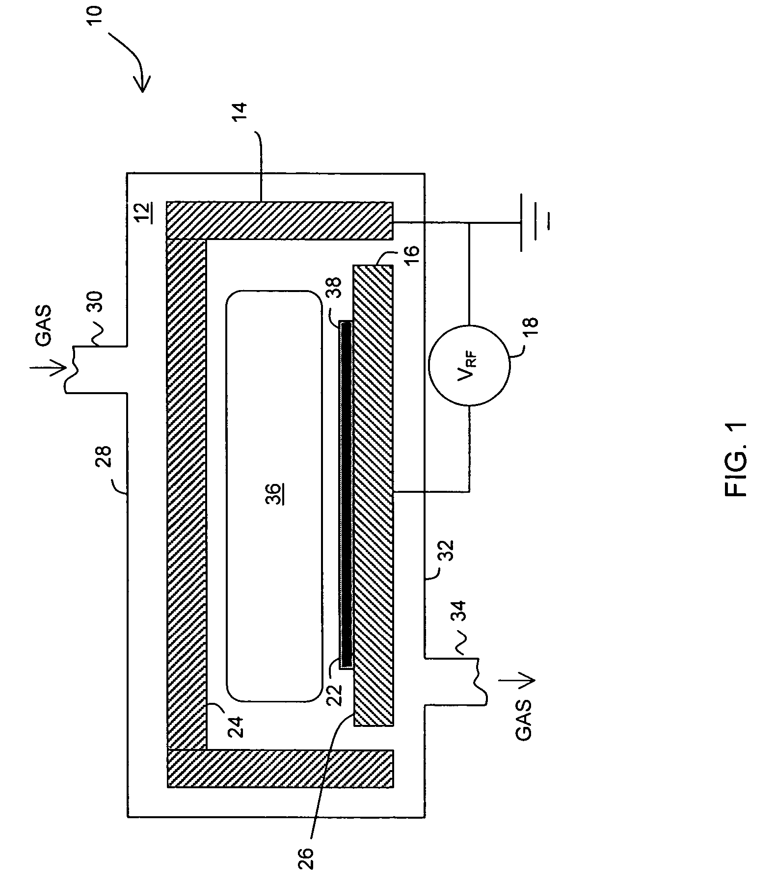
[0014] Referring to FIGS. 1 and 2, a plasma surface activation device 10 is ...


PUM


Abstract

In one embodiment, a method comprises placing a first and a second substrate into a reaction chamber, the first substrate being made of an indium antimonide material and having a first surface and the second substrate being made of a silicon or a silicon dioxide material and having a second surface; exposing the first and second surfaces to an oxygen plasma; forming a bond between the first and the second substrates by placing the first surface in contact with the second surface; and annealing the first and the second substrates to strengthen the bond.

Description

BACKGROUND OF THE INVENTION [0001] 1. Field of the Invention [0002] The present invention relates to semiconductor structures, and in particular, to bonded semiconductor structures. [0003] 2. Description of Related Art [0004] In the prior art, bonding two different semiconductor wafers together, with one of the materials being a semiconductor compound III-V material (such as a gallium arsenide (GaAs) wafer to a silicon wafer), has been accomplished by intermediate “glue” layers, such as spin-on glass or wax. Bonding of these wafers requires an elevated temperature, resulting in large stresses in between wafers upon return to room temperature due to a mismatch in the coefficient of thermal expansion. These stresses often result in the bonded pair of wafers breaking or delaminating at room temperature. [0005] In a prior art plasma bonding device, which is essentially a reactive ion etcher device, a plasma has been used for surface activation, i.e., activation of a semiconductor surfac...

Claims


Application Information

Patent Timeline
IPC IPC(8): H01L27/01H01L27/12H01L31/0392H01L21/30H01L21/46
CPCH01L21/306H01L21/187
Inventor SHAHEEN, MOHAMAD A.LEI, RYAN Z.KELMAN, MAXIM B.
Owner INTEL CORP
Why Eureka
Try Eureka