Low temperature PB-free processing for semiconductor devices

a technology of semiconductor devices and low temperature, applied in the direction of sustainable manufacturing/processing, final product manufacturing, printed circuit aspects, etc., can solve the problems of structural separation of components, new challenges in areas, and components that are unworkable, and achieve the effect of less high-temperature related damag

Inactive Publication Date: 2006-03-02
LSI CORPORATION
View PDF8 Cites 63 Cited by
  • Summary
  • Abstract
  • Description
  • Claims
  • Application Information

AI Technical Summary

Benefits of technology

[0006] The present invention is directed to a bonding agent that allows a solder reflow process to occur at a lower reflow temperature. One area of use includes semiconductor device manufacturing processes where solder materials having high melting temperatures require reflowing. The bonding agent is placed between a solder ball, for example, and a contact surface. The bonding agent is selected to have a melting temperature

Problems solved by technology

These new solder materials are safer for the environment and for electronic device users, however, they present new challenges in areas such as manufacturing.
One manufacturing challenge presented by the new materials relates to their high melting temperatures.
Unfortunately, these components become unworkably soft at such elevated temperatures.
Also, differences between the coefficients of thermal expansio

Method used


Image

  • Low temperature PB-free processing for semiconductor devices
  • Low temperature PB-free processing for semiconductor devices
  • Low temperature PB-free processing for semiconductor devices

Examples


Embodiment Construction

[0016] The present invention will now be described in detail with reference to a few preferred embodiments thereof as illustrated in the accompanying drawings. In the following description, numerous specific details are set forth in order to provide a thorough understanding of the present invention. It will be apparent, however, to one skilled in the art, that the present invention may be practiced without some or all of these specific details. In other instances, well known operations have not been described in detail so not to unnecessarily obscure the present invention.

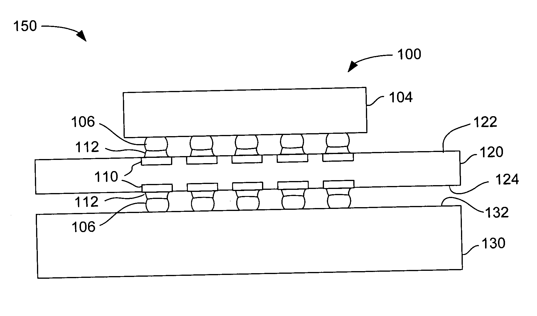
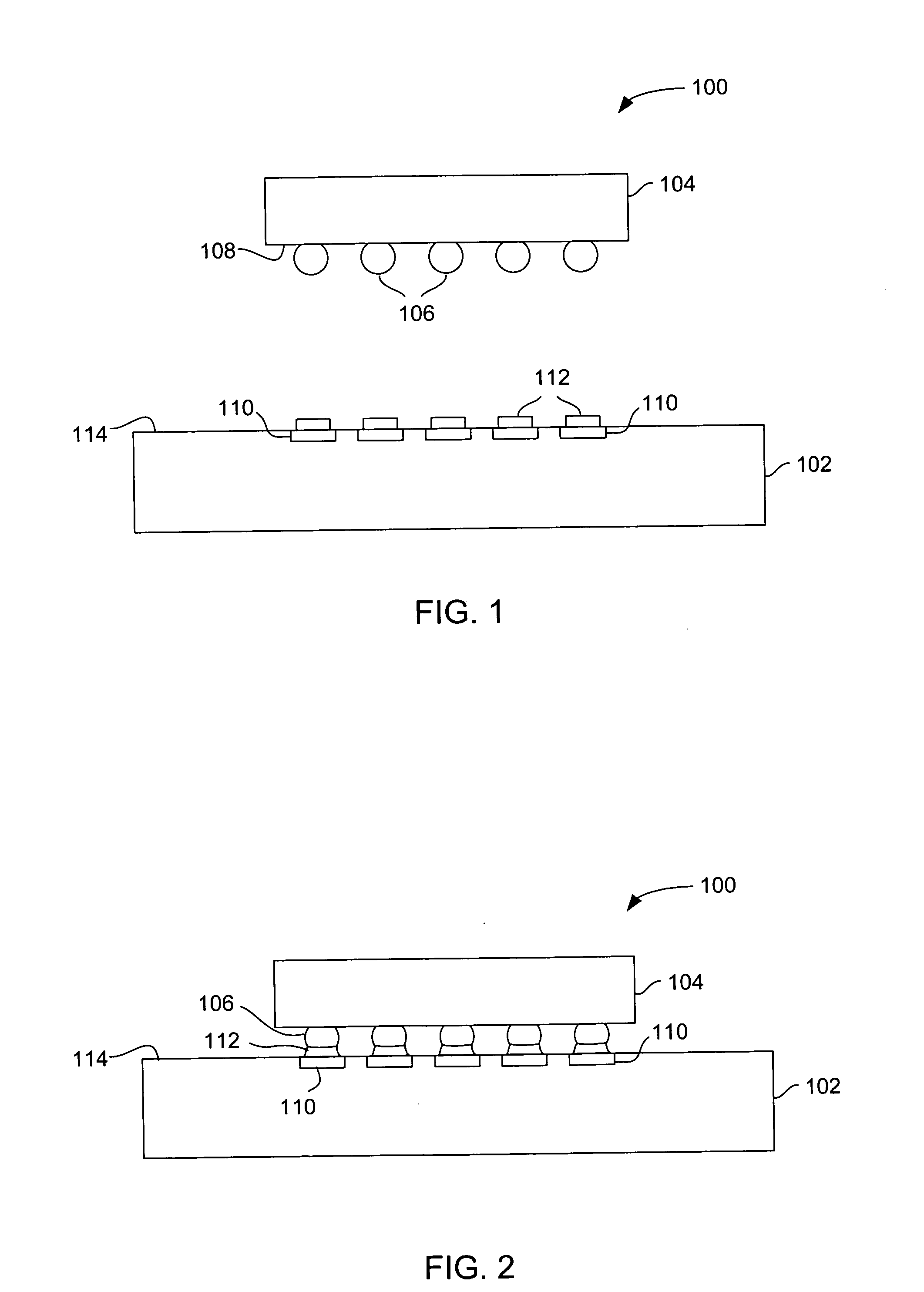
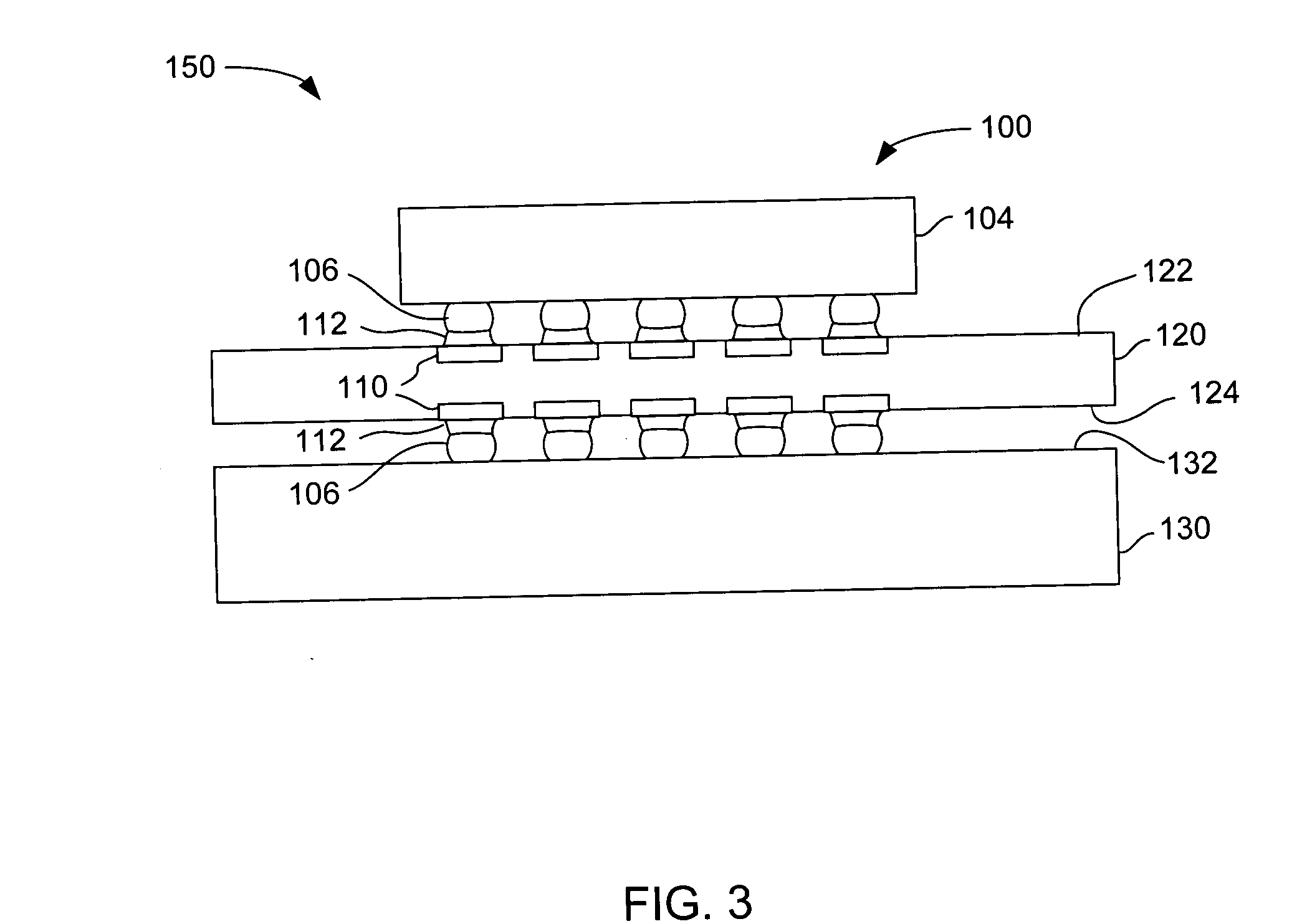
[0017] The present invention pertains to the use of a low melting temperature bonding agent that allows a solder reflow process to occur at a lower reflow temperature. One area of use includes semiconductor device manufacturing processes where solder materials having high melting temperatures require reflowing. High melting typical lead-free solders can be used in conjunction with this bonding agent. The bonding a...


PUM


Abstract

Techniques for utilizing a bonding agent that allows a solder reflow process to occur at a lower reflow temperature. One area of use includes semiconductor device manufacturing processes. The bonding agent is placed between a solder ball and a contact surface. The bonding agent has a melting temperature that is lower than that of the solder ball. Reflow is then performed at a relative low temperature that is high enough for reflowing the bonding agent, yet at the same time, lower than what would be necessary to reflow the solder material. Since, the electrical system is not subjected to the high temperatures necessary for reflowing the solder material, the electronic system experiences less high-temperature related damage.

Description

FIELD OF THE INVENTION [0001] The present invention relates generally to soldering techniques for electronic devices, and more specifically to lower-temperature soldering processes. BACKGROUND [0002] The electronics industry is turning towards lead-free components to reduce hazardous conditions related to electronic devices that incorporate lead components. A common component of the electronics industry is solder material, commonly used in the form of solder balls. Solder balls that contain lead are being replaced by lead-free materials such as, but not limited to, tin, silver, copper, and alloys of such materials such as a tin / silver / copper alloy (Sn / Ag / Cu). These new solder materials are safer for the environment and for electronic device users, however, they present new challenges in areas such as manufacturing. [0003] One manufacturing challenge presented by the new materials relates to their high melting temperatures. For example, Sn / Ag / Cu alloys typically have melting temperat...

Claims


Application Information

Patent Timeline
IPC IPC(8): H01L21/44H01L23/48
CPCH05K3/3436H01L2224/16225H05K2201/10378H05K2201/10992H01L23/49816H01L23/49833H01L24/81H01L2224/81801H01L2924/01029H01L2924/01049H01L2924/01079H01L2924/01082H01L2924/14H01L2924/15311H01L2924/01006H01L2924/01033H01L2924/01047H01L2924/0105H01L2924/014H05K3/3463H01L2924/00011H01L2924/00014Y02P70/50H01L2224/0401
Inventor RANADE, YOGENDRAPARTHASARATHY, RAJAGOPALANHALL, JEFFREY ALLAN
Owner LSI CORPORATION
Why Eureka
Try Eureka