

High-reliable semiconductor device using hermetic sealing of electrodes
- Summary
- Abstract
- Description
- Claims
- Application Information
AI Technical Summary
Benefits of technology
Problems solved by technology
Method used
Image

Examples
first embodiment
[0051] The
[0052] The first embodiment of the present semiconductor device is made by mounting a fist substrate on a second substrate, wherein electrodes formed on the first substrate and electrodes formed on the second substrates are electrically connected via bumps.
[0053] Examples include a semiconductor package in which a semiconductor chip of a Si substrate and an interposer of a Si substrate are connected via bumps.
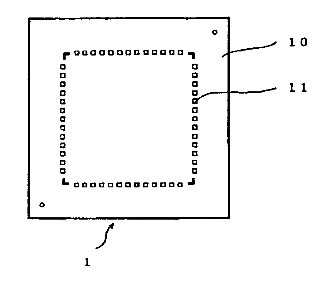
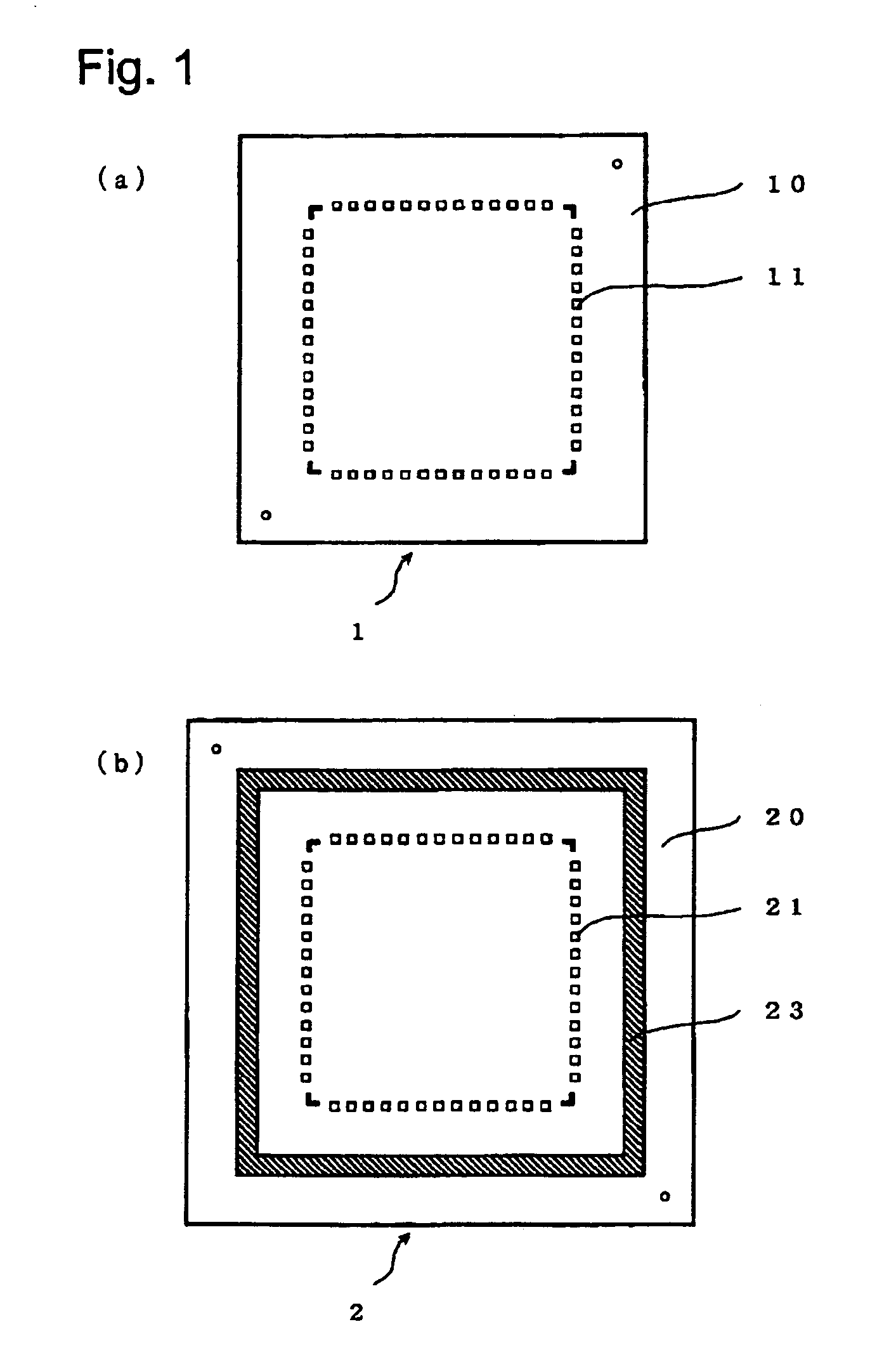
[0054] As shown in FIG. 1(a), on a Si substrate 10 of a semiconductor chip 1, one or more electrodes 11 and other circuits (not shown) are formed by using conventional materials and a conventional process.
[0055] As shown in FIG. 1(b), on a Si substrate 20 of an interposer 2, one or more electrodes 21 and other circuits (not shown) are formed by using conventional materials and a conventional process. A frame member 23 surrounding the one or more electrodes 21 is further formed.
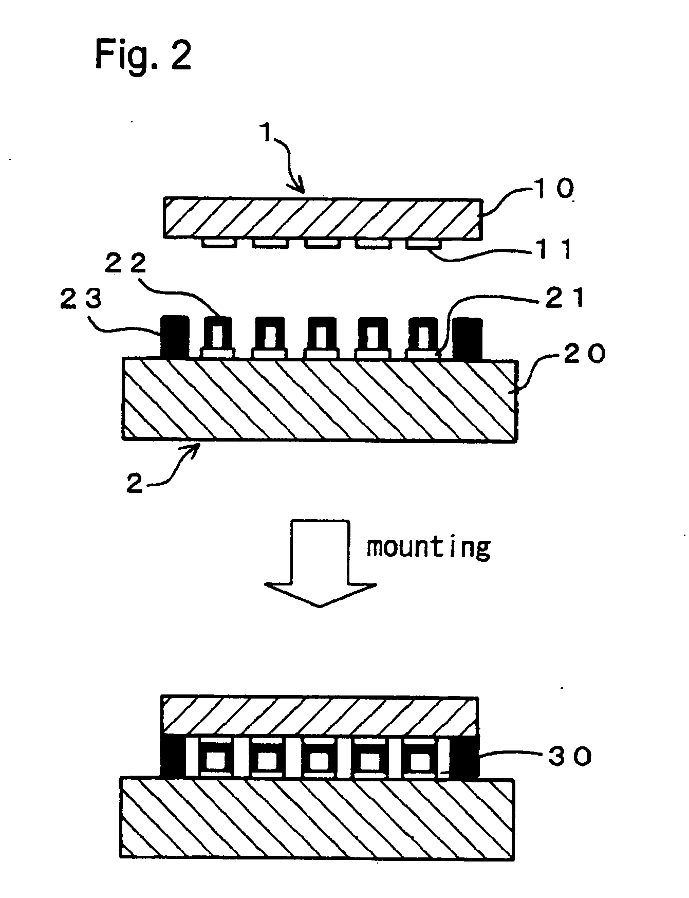
[0056] As shown in FIG. 2, elastic bumps 22 are bonded on each of the one or more electr...
second embodiment
[0077] The
[0078] The second embodiment of the present semiconductor device is made by mounting a fist substrate on a second substrate, wherein electrodes formed on the first substrate and electrodes formed on the second substrate are electrically connected via a bumpless connection.
[0079] Examples include a semiconductor package in which a semiconductor chip of a Si substrate and an interposer of a Si substrate is connected via a bumpless connection.
[0080] As shown in FIG. 4, on a Si substrate 10 of a semiconductor chip 1, one or more electrodes 11 and other circuits are formed by using conventional materials and a conventional process. More specifically, on the Si substrate 10, a wiring layer 16 of a semiconductor element is formed, and an insulating layer 17 is formed thereon. Further, on the insulating 17, a ground wiring layer 18 is formed.
[0081] Through holes are formed through the insulating layer 17 and the ground wiring layer 18, which reach to the wiring layer 16. The el...
PUM
 Abstract
Description
Claims
Application Information