Self-luminous planar display device
a display device and self-luminous technology, applied in the field of display devices, can solve the problems of lowering reliability, deteriorating display quality of display devices, and lowering reliability, so as to improve reliability, improve display quality, and improve reliability
- Summary
- Abstract
- Description
- Claims
- Application Information
AI Technical Summary
Benefits of technology
Problems solved by technology
Method used
Image

Examples
embodiment 1
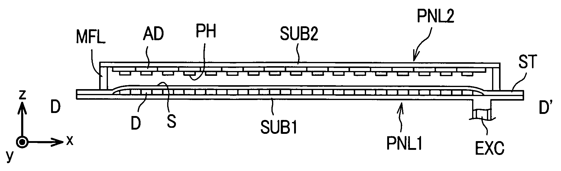
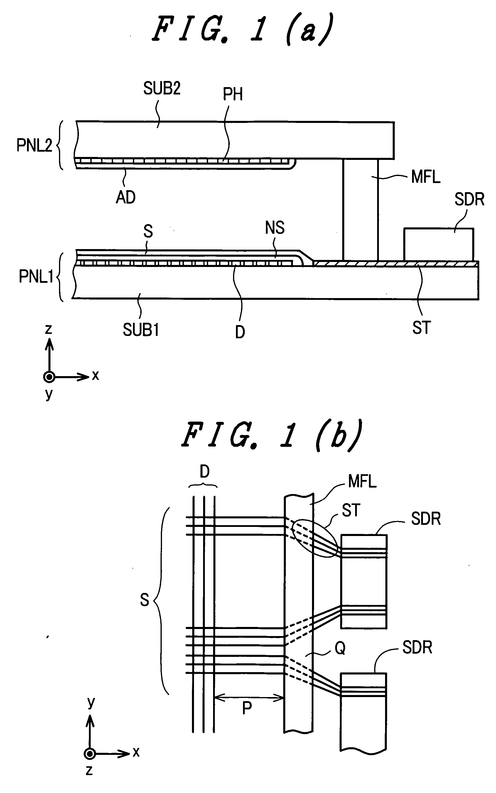
[0043]FIG. 1A and FIG. 1B are schematic views for explaining an embodiment 1 of a self-luminous planar display device according to the present invention, wherein FIG. 1A is a cross-sectional view of an essential part and FIG. 1B is a plan view of an essential part in a state that a face panel is removed from the display device shown in FIG. 1A.
[0044] In the self-luminous planar display device, a back panel PNL1 and a face panel PNL2 are integrally formed using a sealing frame MFL. On an inner surface of the back panel PNL1, a large number of first electrodes (hereinafter referred to as data lines) D which extends in the first direction (hereinafter referred to as y direction) and are arranged in parallel in the second direction (hereinafter referred to as x direction) which intersects the first direction, an interlayer insulation film NS which is formed so as to cover the data lines D, and a large number of second electrodes (hereinafter referred to as scanning lines) S which exten...
embodiment 2
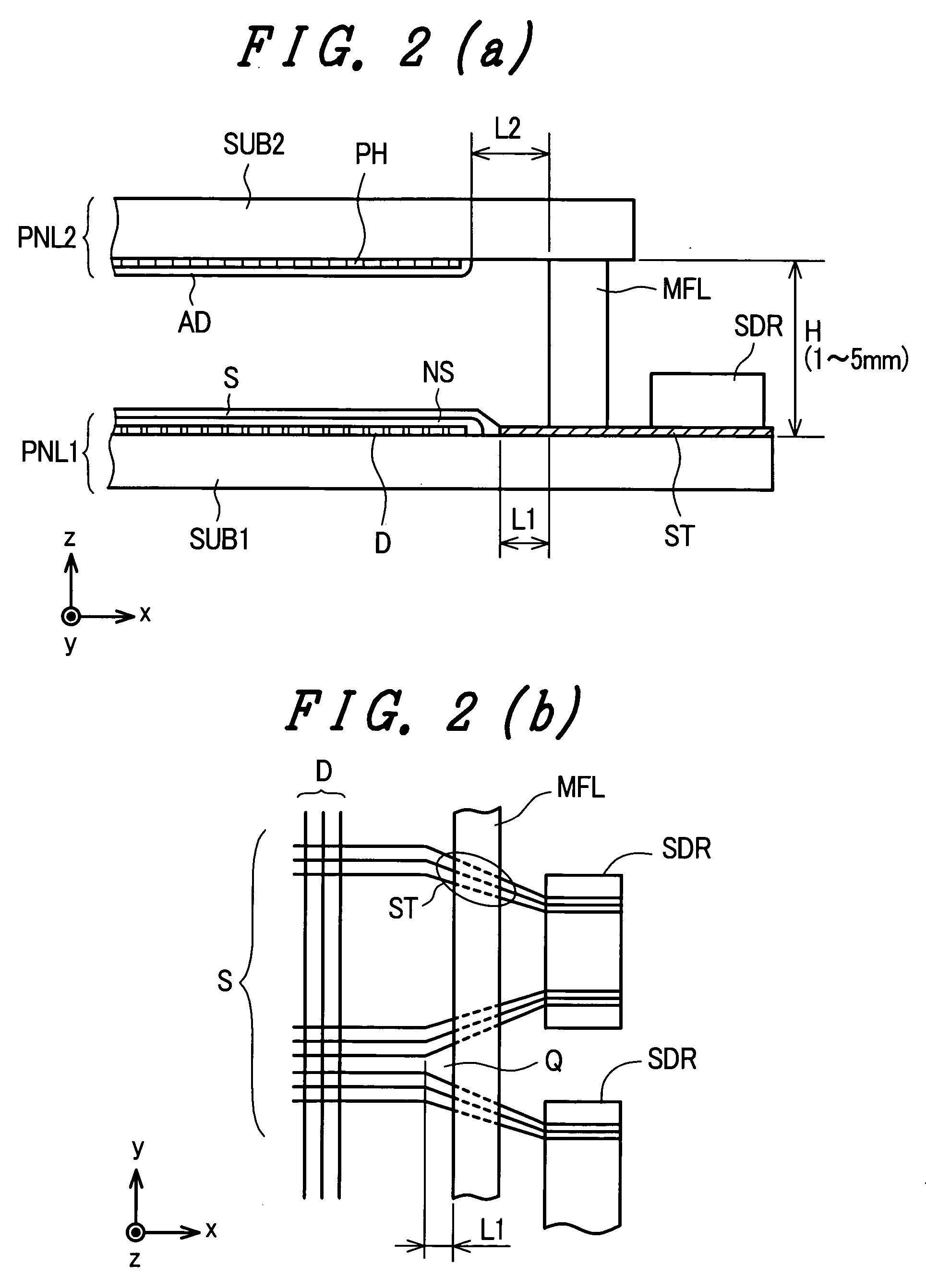
[0050]FIG. 2A and FIG. 2B are drawings similar to FIG. 1 and schematic views showing an essential part for explaining an embodiment 2 of the self-luminous planar display device of the present invention. Although the explanation is made with respect to the scanning line lead terminals ST in the embodiment 2, the embodiment is also applicable to the data line lead terminals. In the embodiment 2, even when the gap Q which is formed by the bending portion is present inside the sealing frame MFL, by determining the total (creeping distance) of a distance from the bent position of the lead terminals to the inside of the sealing frame MFL (a width of the gap Q), the height of the sealing frame MFL, and the distance from the inside of the sealing frame MFL to the end of the anode AD, it is possible to prevent the generation of discharge between the anode and the lead terminals along the surface of the sealing frame.
[0051] That is, assuming a dielectric strength limit value of the sealing f...
embodiment 3
[0055]FIG. 3 is a view similar to FIG. 1B for explaining an embodiment 3 of the self-luminous planar display device and also is a plan view of an essential part. The embodiment 3 is characterize in that with respect to a portion of either or both the data line lead terminals and / or the scanning line lead terminals ST, in the vicinity of the inside of the sealing frame MFL, an enlarged electrode portion R is formed on the bent portion to pull out the lead terminals toward an exteriorly mounted drive circuit. The enlarged electrode portion R covers a gap (portion indicated by symbol Q in the above-mentioned embodiment) which is formed attributed to the formation of the bent portion and hence, the charging area is reduced. It is needless to say that a shape of the enlarged electrode portion R is not limited to the illustrated shape.
[0056] Also with the constitution of the embodiment 3, it is possible to prevent the occurrence of discharge between the anode and the lead terminals along...
PUM
 Abstract
Description
Claims
Application Information
 - R&D
- Intellectual Property
- Life Sciences
- Materials
- Tech Scout
- Unparalleled Data Quality
- Higher Quality Content
- 60% Fewer Hallucinations
Browse by: Latest US Patents, China's latest patents, Technical Efficacy Thesaurus, Application Domain, Technology Topic, Popular Technical Reports.
© 2025 PatSnap. All rights reserved.Legal|Privacy policy|Modern Slavery Act Transparency Statement|Sitemap|About US| Contact US: help@patsnap.com